Previously we explored the very basics of getting a flyback converter up and running, but by the end of it, real world components showed us it wouldn't be so easy after all... But do not despair! Physics may have pulled a fast one on us, but we can use its own tricks against itself.
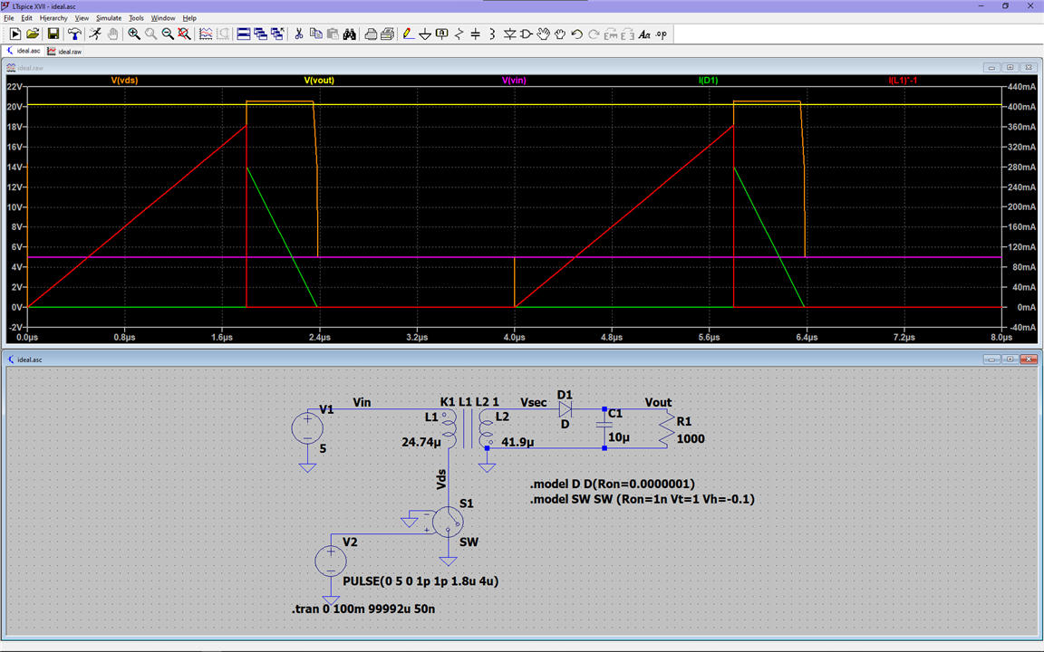
First, we need to understand why that pesky ringing showed up. After some more reading on how to use voltage controlled switches on LTspice, I was able to simulate the circuit from the first blog with components even closer to ideal ones. I also updated the transformer to reflect new measurements, taken after javagoza 's very welcome commments in my first blog led me to further research the modeling of transformers and coupled inductors, thank you javagoza!
In this image we can observe the now properly idealized converter and its waveforms, now also labeled for better clarity:
And to understand why that ringing showed up at the end of the previous blog, we need to understand...
The Flyback Cycle
There are multiple different operating modes for a flyback converter, with the main two being CCM and DCM, and their main defining features are these:
- CCM: Continuous Conduction Mode.
- The current in the transformer never reaches zero during the flyback cycle.
- DCM: Discontinuous Conduction Mode.
- The current in the transformer goes to zero.
This series will focus on DCM due to time constraints, but I'll also briefly show the behaviour of CCM.
What I've been calling a transformer so far is better understood as a coupled inductor. While physically the component we call a transformer doesn't differ much from what we call a coupled inductor, and both perform the task of moving energy from one winding to another through inductive coupling, there is a physically minor but practically significant difference between the two:
In a transformer, the core has no gap in it and the transfer of energy happens continuously, and it is (ideally) not stored in either of the windings but transferred immediately to the load.
In a coupled inductor, the core has a small air gap which prevents core saturation thus allowing for more energy to be stored in the magnetic field. The scope of this series is about making it easy to understand the working principle of flyback converters, and going deep into the details of the magnetics is beyond this, so at the end of this blog I'll leave some links for those who wish to see an explanation of how the gap accomplishes this increase in energy storage capabilities of power inductors. Unlike in a transformer, the energy builds up and is stored in the magnetizing inductance of the primary side during the ON portion of the flyback cycle, and is released to the secondary during the OFF portion of the cycle.
Now our model of an ideal flyback converter will be further expanded to allow us to see its inner workings. In the previous blog I mentioned that Lp should technically be the magnetizing inductance, when showing the output voltage equation:

The updated model of our ideal coupled inductor shows us why

should be used instead:
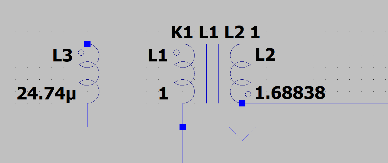
Here I have taken out the magnetizing inductance and replaced the coupled windings with an ideal transformer whose windings have an arbitrarily large inductance for simulation purposes.
In theory, the ideal transformer's windings have an infinite inductance, perfect coupling, and no resistance; for simulation purposes, using arbitrarily high inductances that preserve the turns ratio and don't significantly change the equivalent inductance at the primary is close enough.
With the magnetizing inductance out, considering the primary inductance of the transformer, which would be infinite, would make no sense.
Using this model we can see how the energy is initially stored in the magnetizing inductance during the ON portion of the cycle, and how it is then transferred to the secondary through the ideal transformer during the OFF portion of the cycle:
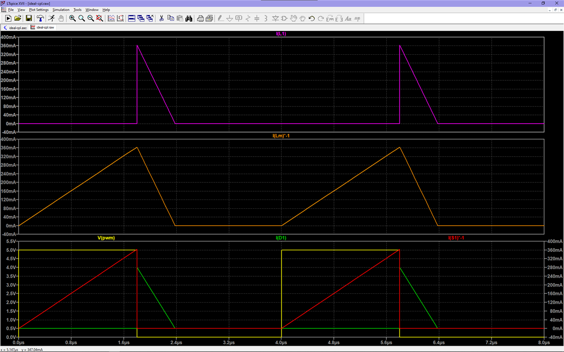
Where L1 is the primary winding of the ideal transformer.
We can see in orange the magnetizing inductance current. It builds up during the ON portion of the cycle, and reaches its maximum as the switch is turned off, then it starts to flow through its only available path: the primary winding of the ideal transformer, and we can see that this portion of the circuit does indeed behave as a transformer, the energy is being transferred immediately from the primary to the secondary.
Considering the entire system, its behaviour is that expected for a coupled inductor, as we see current flowing through the switch during the ON portion of the cycle, and abruptly stopping during the OFF portion. This is better illustrated by the following diagram:
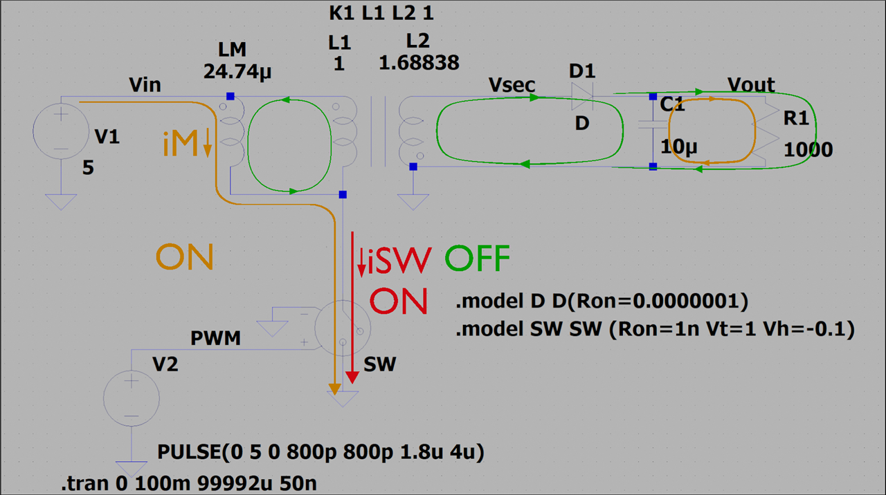
Seeing this diagram you may wonder why current isn't flowing through L1 during the ON portion of the cycle. Consider that for current to flow through it, since it is perfectly coupled to L2, current would have to flow through L2, into the dot at L1, and out from the dot at L2, but it can't because of the diode, so during the ON portion of the cycle, all the current on the primary side only flows through LM and through the switch, and in steady state operation, current also flows through the load resistor thanks to the energy stored in the capacitor.
You may also have noticed two other terms not explained in the output voltage equation. These terms, D and T, are the duty cycle and the period of the switching frequency, respectively. D is the ON duration as a proportion of the period T.

Now that we understand what the flyback cycle is, and how our circuit behaves during the cycle, the next step in understanding why there is ringing is to look again at the
Real circuit implementation
As previously determined, real life components are always less than ideal, and in many cases, far from it, so let's build the real life imperfections into our ideal circuit and see how things start changing. To begin with, let's consider the leakage inductance of the transformer and the capacitances of the MOSFET.
Previously, I was taking into account the entire leakage inductance as seen on the primary and secondary windings, but I was also shorting the auxiliary winding of the transformer. javagoza correctly pointed out that this leakage shouldn't be considered if that winding was not to be used. This is because that winding isn't loading the circuit in any manner, and thus it wouldn't matter how its coupling affected the other windings. Upon reading about leakage measurement procedures, I came across omicron lab's transformer modelling application note, and from it and the measurement results with the shorted windings, I gathered that the leakage inductance measured this way was actually the total leakage as referred to the winding being measured, which was later confirmed when watching This video by Biricha on Youtube. This means we only need to measure the primary winding leakage inductance while shorting the windings we will use. In my case, only the secondary will be shorted.
From that application note I also learned that the measurements should be taken at frequencies at which the parasitic capacitances are not loading the circuit, which can be seen during measurement as when the impedance slopes stop being linear:
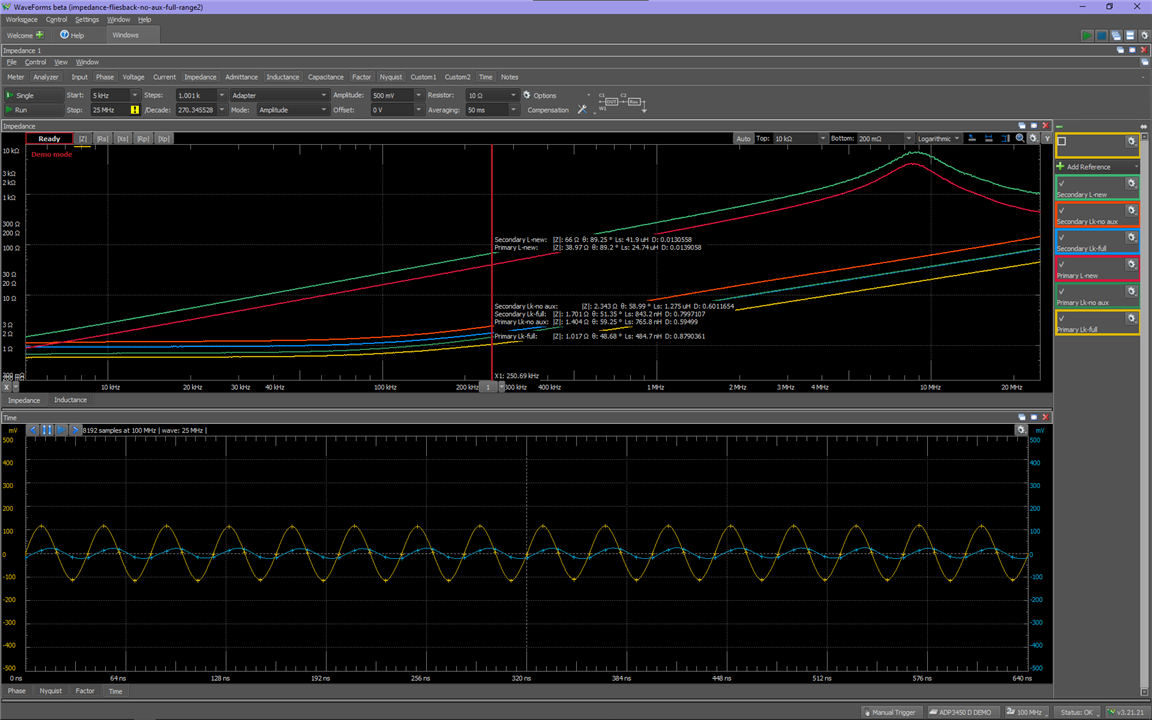
so in this case, up to about 2MHz.
This can also be seen in the sharp increase in inductance after that point:
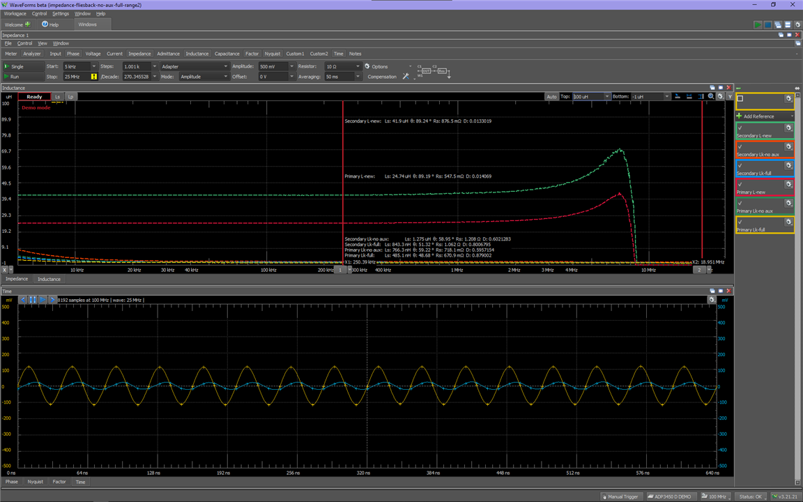
The application note will be linked at the end for those interested.
So with this in mind, the new circuit, considering leakage inductance, series resistance, and MOSFET capacitances, looks like this:
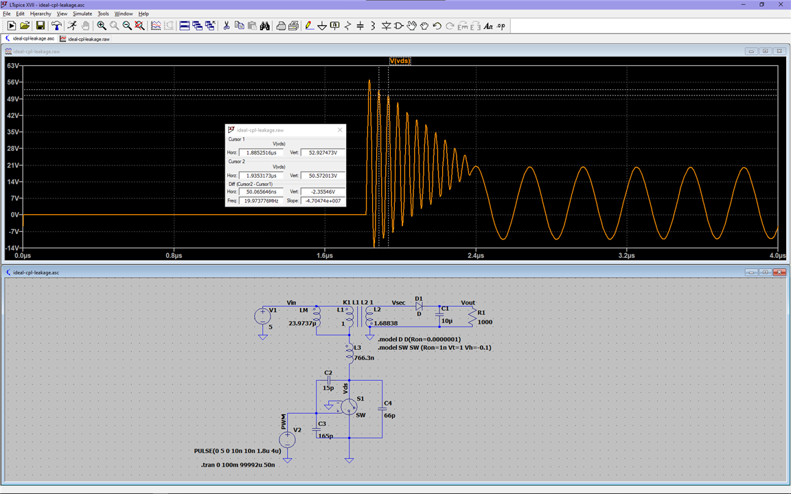
We can see those changes alone resulted in the massive ringing upon entering the OFF portion of the cycle, but why do they happen?
Essentially, when the switch is ON, those capacitors are shorted, and there's energy stored in the leakage inductance. When the switch turns OFF, the current flowing through the leakage inductance wants to keep flowing, and now the capacitors of the MOSFET are not shorted and behave like, well, capacitors, and together with the leakage inductance they form a series LC resonant circuit, offering a path for the current to flow equivalent to this:
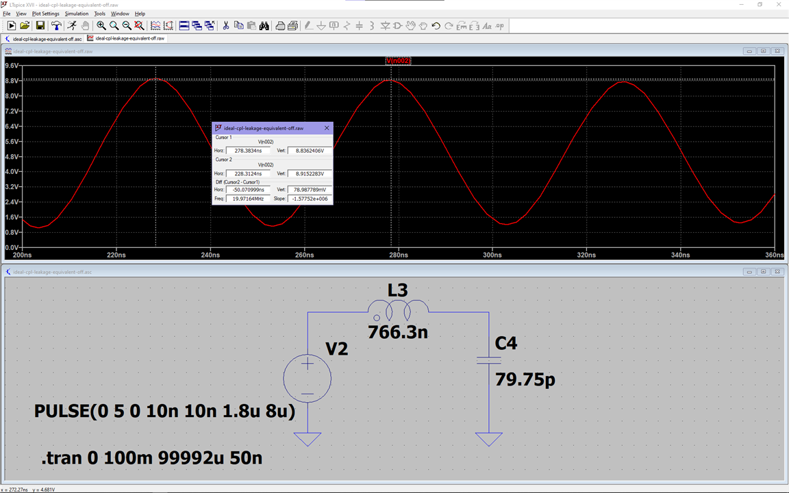
Now, what about that other lower frequency ringing we see after the magnetizing inductance has ceased conducting?
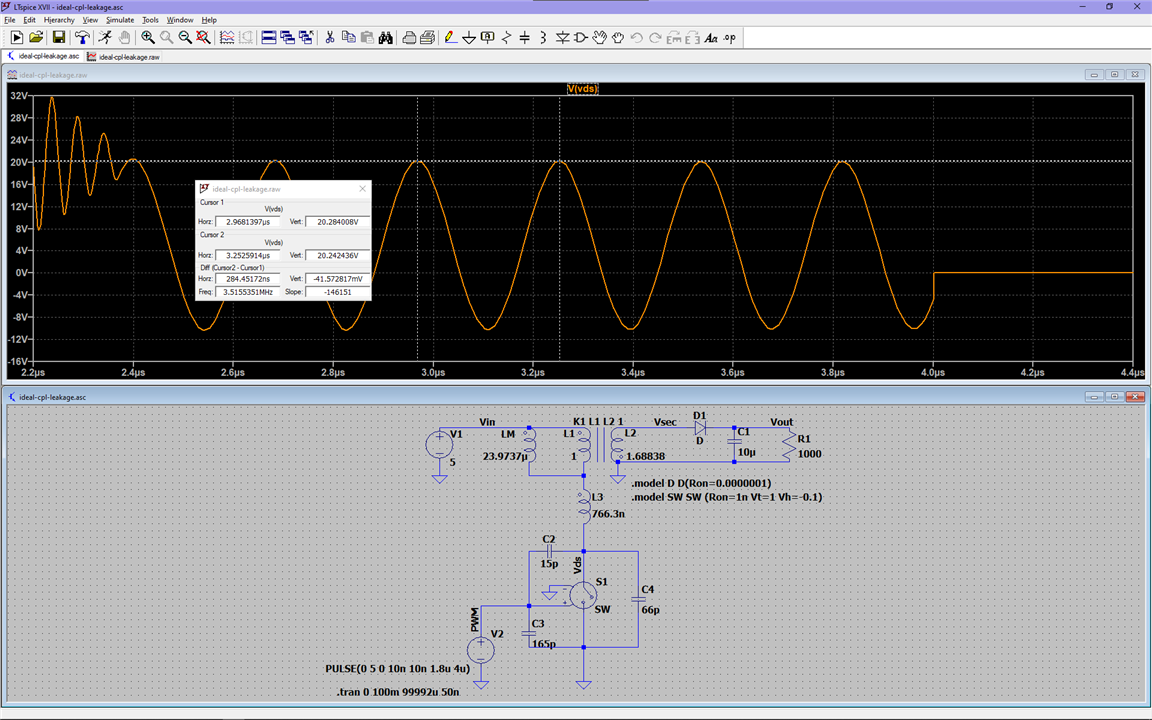
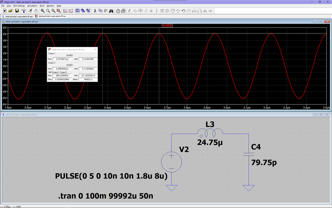
While there's still current flowing through the magnetizing inductance and the primary of the ideal transformer, only the leakage inductance resonates with the capacitors of the MOSFET, but once all the energy is transferred to the secondary, the magnetizing inductance is added to the leakage inductance in series, and becomes part of the resonant circuit, and so, the equivalent circuit becomes this:
Great! We now understand where the ringing comes from, but why do we care? The circuit still works fine like that after all.
Looking at the image where I added the less-than-ideal parameters, leakage inductance and MOSFET capacitances, we see there are massive voltage spikes across our would-be MOSFET, and while that's not a problem for our perfect simulated components, when it comes to designing for the real world, we're stuck with our ESD sensitive, absolute maximum ratings, heat-dissipating, riddled with parasites, components, and we need to accommodate their needs.

While for this particular example the voltages are still low enough that they won't harm our components, it is important to consider the general case, where we might be dealing with Vin in the hundreds of volts, or where the output is not in the 10 to 20V range but in the 50s or hell, the 500s, because let's be honest, when you hear flyback, you think about mad scientist contraptions that shoot sparks or that TV that almost killed poor cousin John on that fateful night!
So what do we do about it?
There are multiple different methods we can use to reduce the ringing and voltage spikes at our primary side switch. This blog will cover only RC snubber on the primary side. Links at the end of the blog for those who wish to further explore this topic.
The RC Snubber
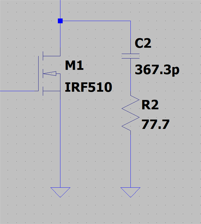
From its name, and *those guys* in this blog's banner, it's no surprise that the RC snubber is just a capacitor in series with a resistor. What may not have been obvious is where that RC network should be located within our circuit.
Previously, I drew the equivalent circuit of the components responsible for the ringing observed across the ideal switch with the MOSFET capacitances. Those capacitances are not constant across all possible operating parameters and were used just to illustrate how they, together with leakage inductance caused the ringing.
LTspice appears to consider the changes in capacitance, and the ringing frequency when using those more realistic components is around 16MHz
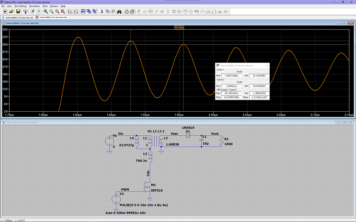
Since we know the frequency and inductance, we can determine the new total capacitance the circuit sees when the MOSFET is OFF using this equation:

Now, as equivalence was demonstrated, I will use the much faster to simulate LC equivalent circuit from before, using the new capacitance value:
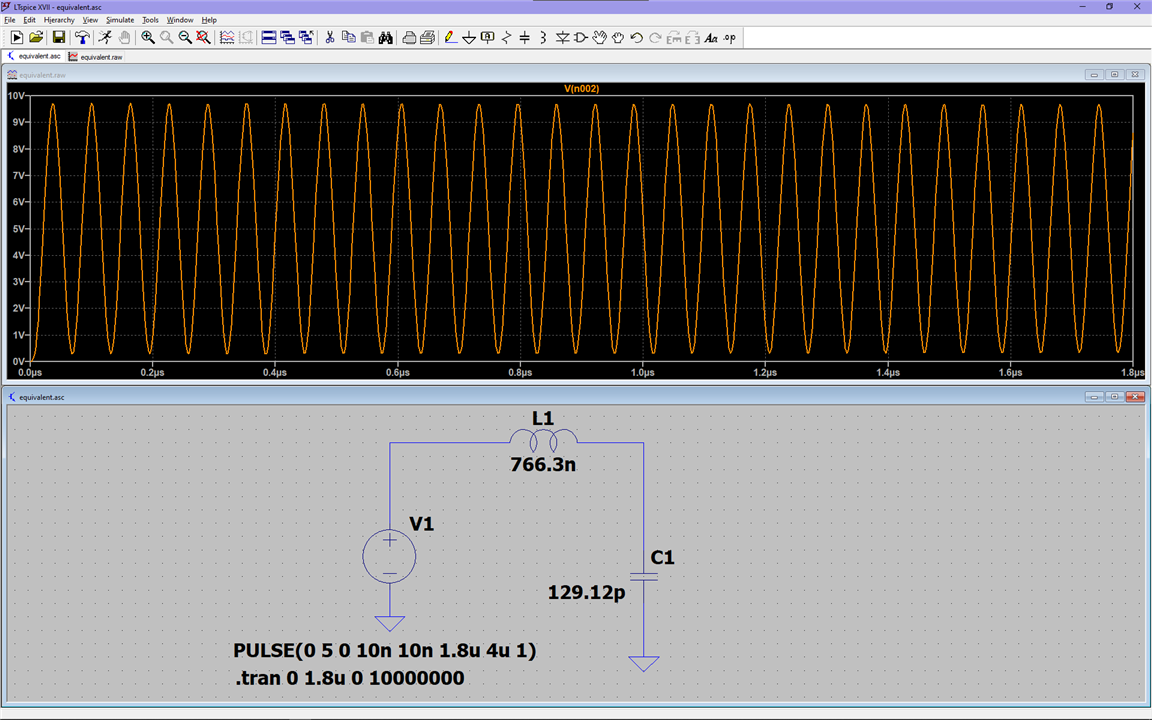
The goal of the snubber is to reduce that ringing as much as possible. In this simulation, the ringing never stops because as there is no resistance, the energy isn't dissipated. We want to take that energy away from the resonator, and the best way to do that is through a resistor:
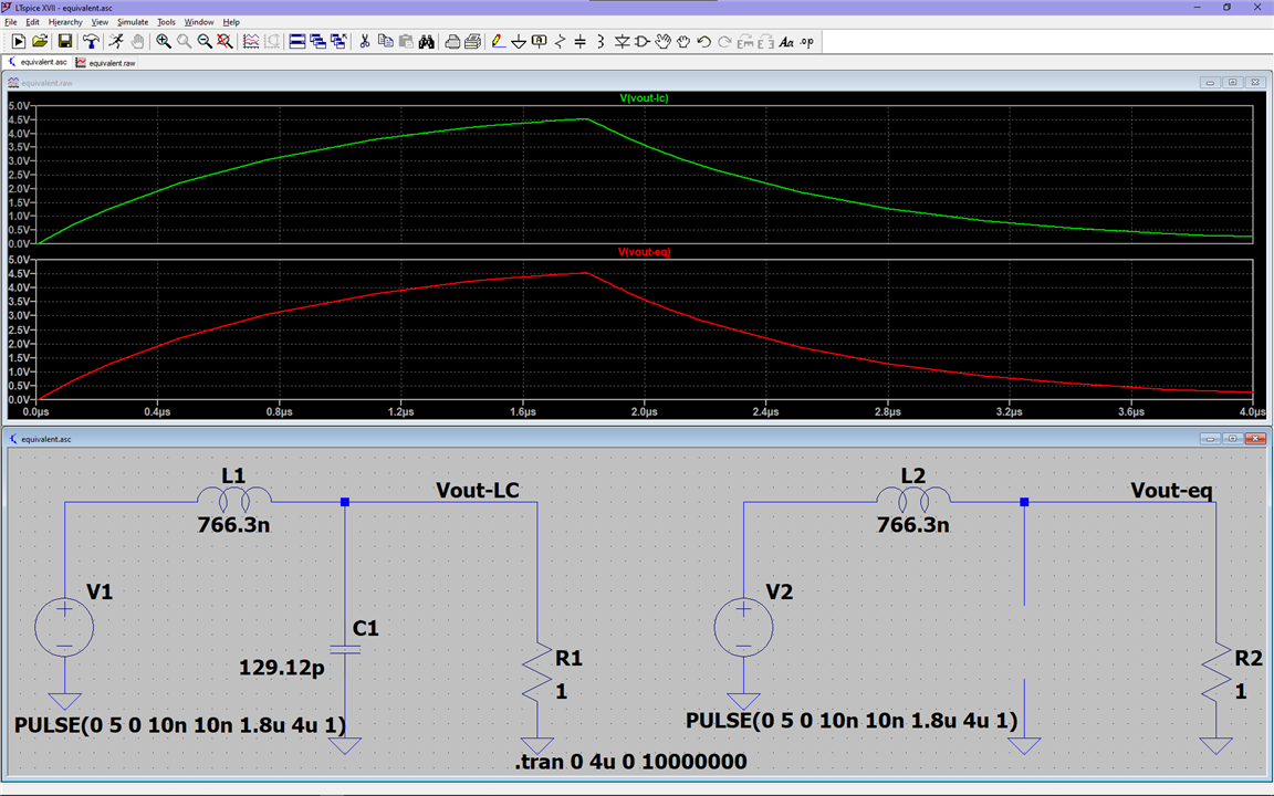
Using a 1 ohm resistor is very effective at removing the ringing, but this has also completely distorted the waveform beyond any usability, and this also has the disadvantage of being in a constant conduction state.
Note:
We know the magnitude of the impedance of a capacitor is calculated like this:
From this, it's clear that the capacitor's impedance is significantly higher than that of the resistor, and so, the resistor becomes dominant enough in the circuit that having nothing instead of the capacitor would be equivalent, and this is also shown in that simulation screenshot.
If we were to use a simple resistor in our actual flyback converter circuit, that resistor would provide a constant path for the current to flow through from the magnetizing inductance back to the DC source, so barely any energy would be stored, and the flyback converter would be useless:
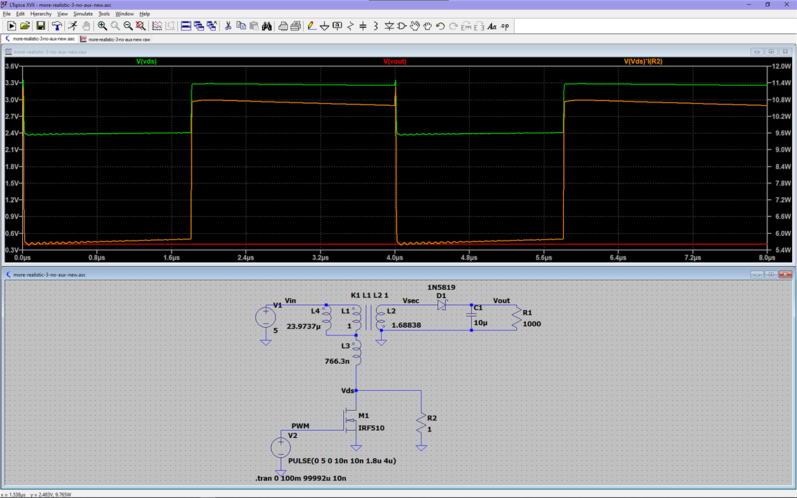
Unless your goal is to make an 8W heater that happens to provide 400mV to a 1k resistor, we need to stop the current flowing through the resistor when the MOSFET is ON.
This is accomplished with a capacitor in series. This capacitor will have a high impedance at the switching frequency, allowing the energy to be stored in Lm, and a low impedance at the ringing frequency, allowing the snubber resistor to dissipate the energy stored in the leagake inductance. It will also set how much power is dissipated by the snubber resistor. so how do we pick this capacitor, and a proper value for our resistor?
This is a blog about experimenting with flyback transformers and all I've done this far is ramble with simulations, so I'll get to it:
We set an acceptable power to be dissipated by the resistor, then:

And for the resistor:

This is from another video by Biricha that explains the entire process.
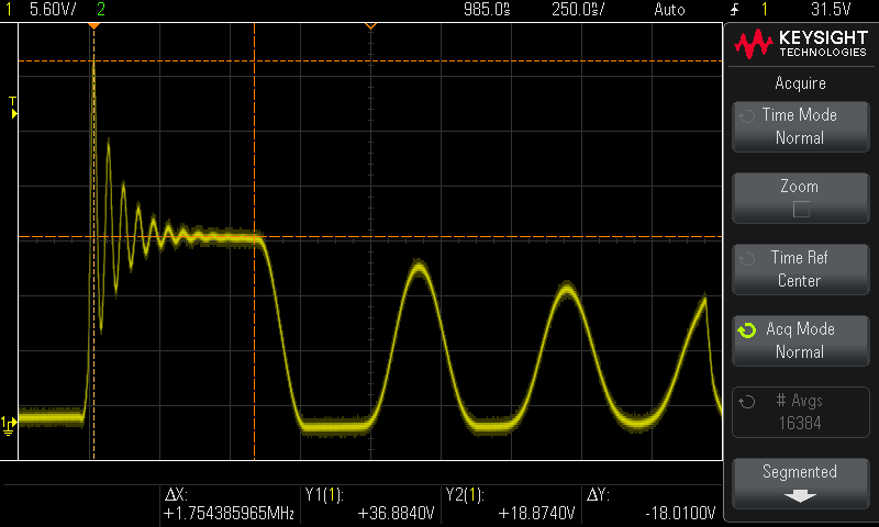
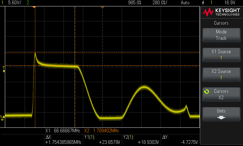
Simulation? not this time, let's see how the real circuit does:
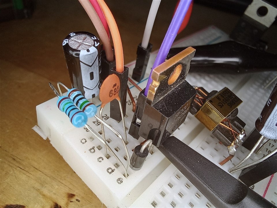
A before shot:
And after!
Fine, I lied, I can't resist a good simulation, especially when reality matches it almost perfectly:

Simulation values were adjusted to match the values of the real measured components.
We still see a voltage spike, which, again, is not harmful at these voltages. However, it's always good to consider the general case, as we never know what we'll have to design for in the future. And in the future, too, lies what we can do about that spike: Clamp it down!
Now, here are the links to the resources mentioned throughout the post:
Gapped, ungapped, and distributed gap toroids in power electronics
Why the Ferrite in an air gapped core?
ElectronicBits#22 - HF Power Inductor Design
Step-by-step Snubber and Clamp Design for Power Supplies
Bode 100 - Application Note Transformer modelling
Flyback Converter Voltage Equation in Discontinuous Conduction Mode (DCM)
Flyback Converter Average Magnetizing Inductor Current
As before, all feedback is welcome.
Thank you!


