Having built the boards, I was determined to get one running before Christmas.
It went quite well.
The first tiny snag, that wasted a little time, was wondering why the 3.3V regulator (LM1117) was only outputting 3.0V. It turned out that with no load at all (I’d left the jumper off for the first power up) the LM1117 doesn’t actually regulate properly – and rather surprisingly gives out less than the expected voltage.
Once it had a load it was OK.
The next snag was that the undervoltage reset chip was not coming out of reset. That was my fault for fitting the wrong part! I’d forgotten that I have both 3V and 1.6V parts and had fitted the wrong one – easily enough fixed.
Then the big snag occurred. Efinix, in common with Gowin and others, don’t make their own programming interface hardware but recommend an FTDI Mini-module (2232 or 4232). They show exactly how to connect it up and have some good notes (explain what to do and it works) to get it running.
I’d bought 2 Mini-modules a couple of months ago from a big name distributor (not Farnell !) and I wired one up. It wasn’t quite the same as the picture on the FTDI datasheet (TQFP chip rather than QFN) – and worse – it didn’t work, Windows couldn’t detect it, and neither could FTDI’s scan and tweak utility. The other module was just the same.
After a bit of stamping about and cursing, I remembered that I had another module connected to a Gowin board (bought a year os so ago from Farnell), so I dug that out and it not only looked like the data sheet, but it worked as well!
On closer inspection I realised that the non working Mini-modules recently bought from XXXX were made in 2010 – so I won’t be buying any more from them!
Effinix’s programmer app is about the easiest to use that I’ve seen (in the FPGA world) and their support documentation is pretty good – way simpler than Intel/Altera or AMD/Xilinx but definitely adequate.
I needed to write some code for the dev board processor to boot the FPGA (ie to make it load its ‘code’ from the external serial flash into its operating RAM).
Then I tweaked a tiny LED blinker I’d already written for an Efinix T8 board to run on the T20 on my dev board. The Efinix software makes changing the type of FPGA a good deal simpler than I’m used to.
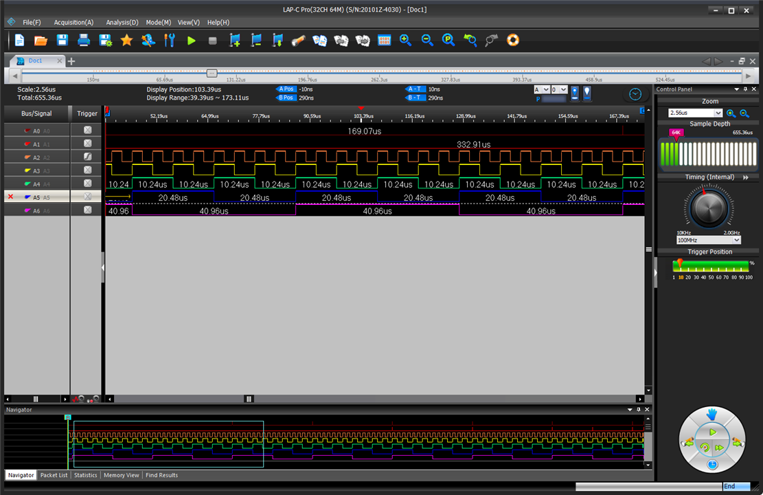
There are not any LEDs on the Dev board, so I used the logic analyser instead.

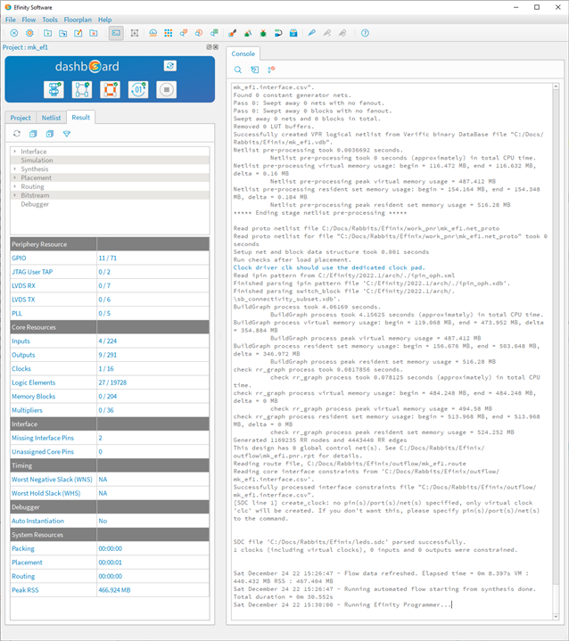
Efinix development tool output as it build my simple test code

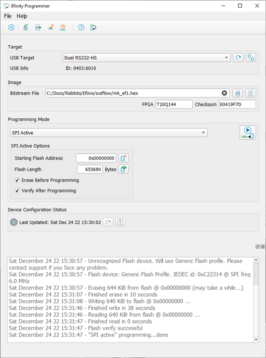
programmer dialogue as it burns the hex file into the serial boot flash for the FPGA

Dialogue (via Hyperterminal) with my code on the dev board processor to get it to boot the FPGA

Logic analyser output showing the test count pattern on 5 output pins
Debugging set up.
The good news is that the whole chain from VHDL to FPGA is working. The 25MHz clock is getting into the FPGA and the on-board processor can boot it.
Next thing is to write some more serious FPGA code to get those PSDRAMs going. And then - get the whole thing doing something useful.
But before that I have to cook a turkey.
MK
