


For all the parts to this project, click here! Smart Doorbell System
Introduction
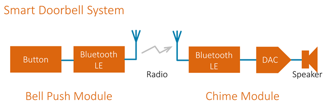
The Smart Doorbell System is an idea for a wireless and portable bell-push/chime system with better range and features than expected from existing systems!
This blog post concentrates on the printed circuit board (PCB) design of the bell push, and the chime module. Read on to find out more!

The high-level block diagram below shows what is being implemented. If you’re interested to know more about the doorbell project then click the link above to all the earlier parts of the project which cover the details such as the circuit schematics otherwise read on here, to see the PCB design considerations.
Brief Overview
The bell push module consists of a Texas Instruments CC2640R2 chip (which contains a microcontroller and Bluetooth LE wireless capability), and a microswitch push-button, antenna, and the battery. The bell push schematic was discussed in part 5.
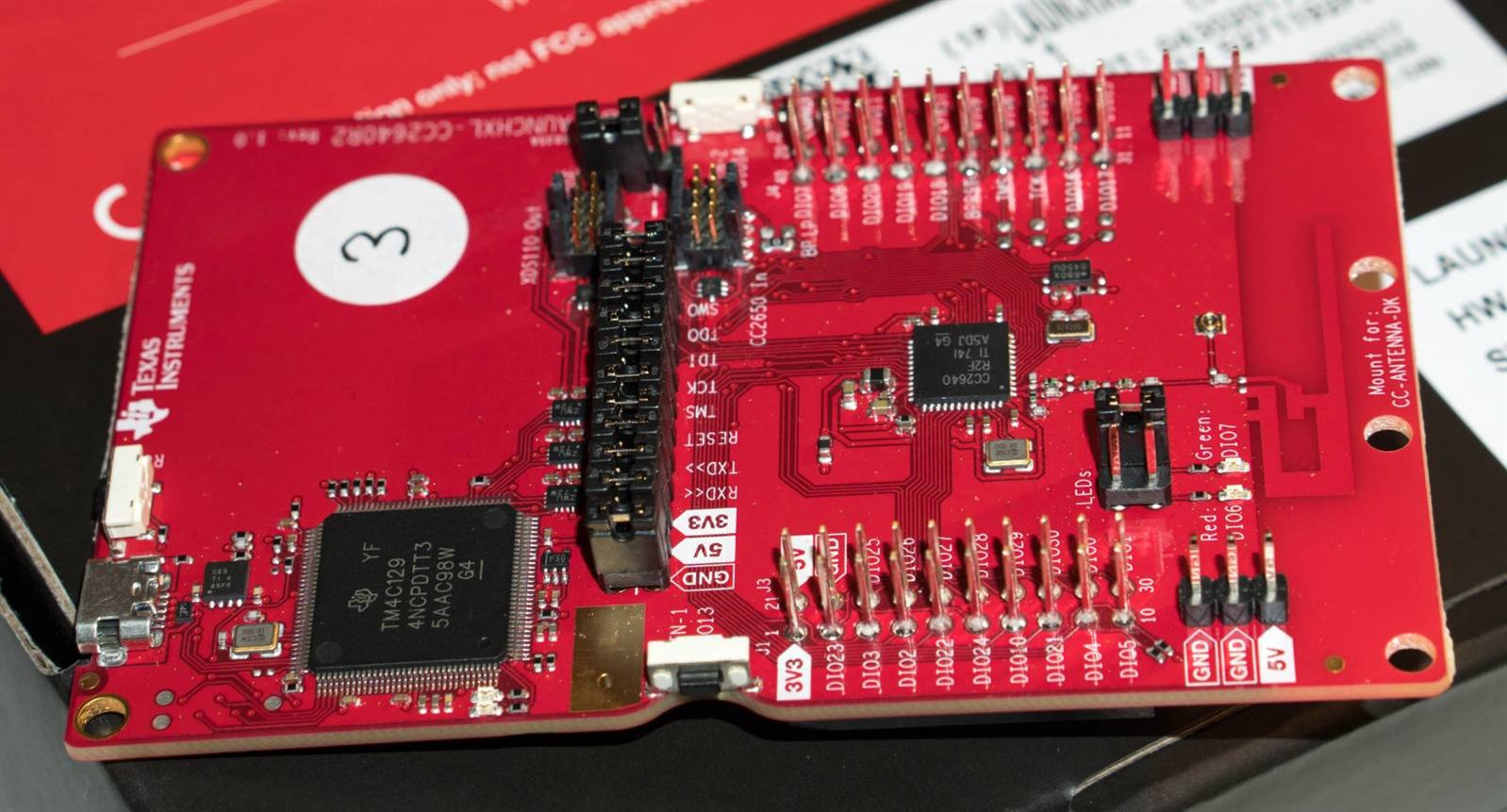
The chime module also uses the same chip, but on a ready-made development board from Texas Instruments, called the CC2640R2 LaunchPadCC2640R2 LaunchPad as shown in the photo below.
The chime module consists of a plug-on board that will fit on top of the LaunchPad. It will contain the audio tones/chime circuitry, audio amplifier, and battery charger (so that the chime module can be used indoors or outdoors).
For the chime module, it was decided to create a plug-on daughterboard with a digital-to-analog converter (DAC) for audio chime sounds, an audio amplifier, and also a battery charger. The chime module circuit was covered in part 6.
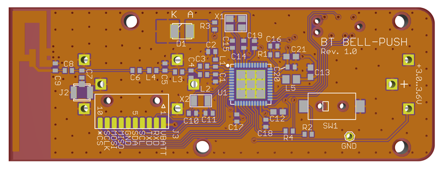
Chime Module Daughterboard
The daughterboard was designed to plug on top of the CC2640R2 LaunchPad, but to leave the antenna portion of the LaunchPad exposed.
There was plenty of board space, and I considered adding things like an LCD screen, but decided against feature creep for now, tempting though it was.
The technique I used was to obtain measurements of the LaunchPad from Texas Instruments design documentation, but also some measurements were taken directly from the Gerber files. Next, the components were placed in approximate desired locations, and the logical connections (known as airwaves) were manually routed. After that, I took a step back, and unrouted some areas, moved some components around, and then pretty much re-routed everything again manually, ripping up each track into an airwave first of course. My brain needs two passes at it, others may be able to achieve better results in one pass : ) There are some screenshots of the results of this mental process near the end of this blog post.
Next, I took another look at the design and did any final rotations and moves of components, and tidied up the traces in those areas. Text objects were moved around, so that they did not clash with vias.
It is very important to run error rules checking and design rules checking, basically use as much of the CAD software features as possible to try to eliminate errors.
Gerber files were then generated, and inspected in a third party 3D viewer, and this visually revealed all the areas where traces could be made neater, and all the areas where text may still be badly located.
After a few iterations of some of these steps, this was the final result:
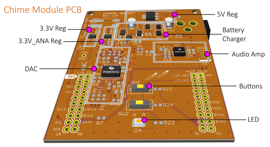
There are two buttons and an LED that will form the user interface along with the speaker. Here is a closeup of the front of the PCB:
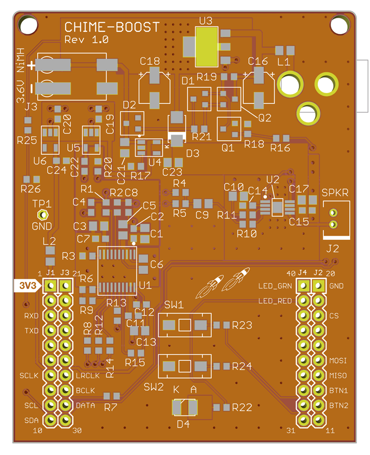
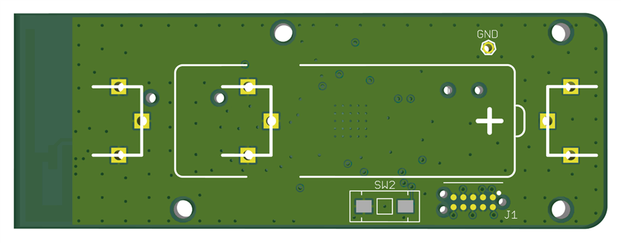
The underside has less features; nothing is mounted on this side apart from the two 20-way dual-in-line (DIL) header sockets, and the DC power socket:
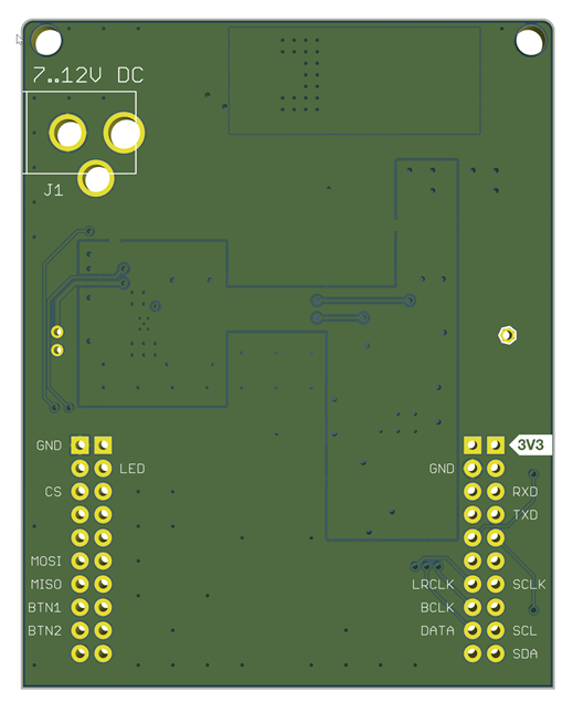
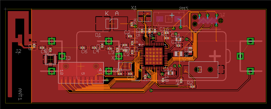
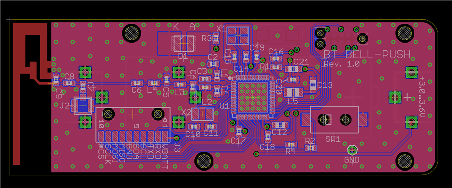
Bell Push Module
The Bell Push module circuit diagram was discussed in Part 5. It is a simpler circuit than the Chime Module, but requires a more complex PCB and more intricate assembly. A 4-layer PCB is used by Texas Instruments. I decided to do the same thing, to have a completely solid ground plane layer. Furthermore, the CC2640R2F chip is in a tiny QFN package so it won’t be as easy to solder, nor will the tiny 0402-sized resistors and capacitors. The chime module used much larger parts. For the wireless design, the size of the components will matter, and therefore the tiny 0402 sized parts are preferred.
The PCB is fairly compact at 77x28mm. There is the possibility to reduce it further in subsequent revisions, and replace some components for reducing the size further, but I felt this was small and usable enough for this first iteration, as a proof-of-concept. My current existing home doorbell button has external case dimensions of 80x32mm so it is comparable. The current one uses a smaller battery so its depth is less though.
It can be noticed that the microswitch in the design is not centered, nor is the LED. The microswitch does not need to be centered, because a lever can be used to actuate it. This could be a piece of springy plastic positioned behind any circular plastic button piece. In a similar vein the LED does not need to be centered because plastic light pipes or lenses could be used to get the illumination to the desired area.
The 28mm dimension is determined by the size of the antenna, so for a narrower design a different antenna design would be needed. The 77mm dimension is mainly determined by the length of the AA sized 3V Lithium battery plus the metal battery clips; thinner clips are possible to shave a few more millimetres. A smaller battery could be used too.
The 28mm width will also affect the antenna behaviour; a slightly larger ground plane is desired for the selected antenna, but this bell push module needs to be fairly small, so it is a compromise. There is the possibility of increasing the ground plane size with a partially metal enclosure, although then the antenna matching components would need to be adjusted.
Lots of ground plane stitching was used; there is a formula for such stitching, based on the radio frequency of operation and hole size, but I followed the TI LaunchPad design since it is a known implementation.
All components are placed on the top side, except the battery clips and the button to pair the bell push module to the chime module. The negative end battery clip can be soldered in one of two positions, to test this board with either AA or 2/3 AA sized cells.
Iterations!
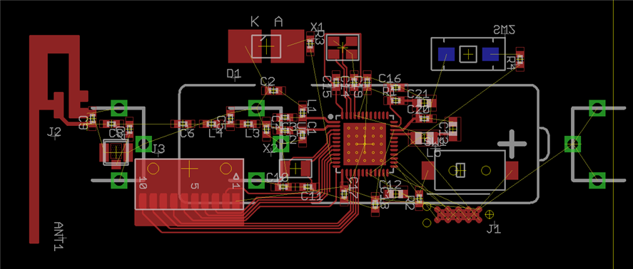
As a mini-appendix, I thought it may be interesting to document what some of the PCB design iterations looked like in EAGLE. When I started creating the PCBs, I placed the parts as best as I could, and laid down lots of tracks, but then ripped them up and moved some parts around, and then redid the tracks, and then ripped them up a third time for near-final tweaks.
Here is what the bell push module PCB looked like at an early stage; most of the tracks are laid down, but a few air-waves (thin yellow lines which represent connections still to be made) still exist:
I moved a few parts around (in particular, the debug connector) and put down a ground plane. The LED pads have been moved slightly too. There are many minor positioning adjustments too, for the passive components. The highlighted orange traces below are the ones that are violating design rules:
And here is the final result, after adding some holes, and correcting the design rule errors, and tidying up the text too. Notice that nearly all the tracks that were laid down previously, have been ripped up and moved slightly to be tidied up.
Summary
The chime module PCB is a two-layer design that will plug on top of the Texas Instruments development board, to construct the entire chime module.
The bell push module PCB is a tiny 4-layer design that will form a complete standalone module with a battery plugged into the back of it.
The designs will be submitted to the PCB factory after 24 hours! This period is critical to allow me to re-examine the designs, and do a self-review of it all, to try to catch any errors and correct them first. Although time is short (and I’ve learned that taking a couple of weeks out in Florida can slow you down a lot!!), I’ve been burned before, even the simplest designs can have faults if one is too hasty. For a real commercial design, formal reviews should take place. Extra pairs of eyes can catch so many issues. Minor problems can be patched with wires on the first prototype, but I want to reduce the risk of that as much as possible first. Thanks for reading and following the project so far!
Top Comments