element14 Community
element14 Community
    Register Log In
  • Site
  • Search
  • Log In Register
  • Members
    Members
    • Benefits of Membership
    • Achievement Levels
    • Members Area
    • Personal Blogs
    • Feedback and Support
    • What's New on element14
  • Learn
    Learn
    • Learning Center
    • eBooks
    • STEM Academy
    • Webinars, Training and Events
    • More
  • Technologies
    Technologies
    • 3D Printing
    • FPGA
    • Industrial Automation
    • Internet of Things
    • Power & Energy
    • Sensors
    • More
  • Challenges & Projects
    Challenges & Projects
    • Design Challenges
    • element14 presents
    • Project14
    • Arduino Projects
    • Raspberry Pi Projects
    • More
  • Products
    Products
    • Arduino
    • Dev Tools
    • Manufacturers
    • Raspberry Pi
    • RoadTests & Reviews
    • Avnet Boards Community
    • More
  • Store
    Store
    • Visit Your Store
    • Choose Another Store
      • Europe
      •  Austria (German)
      •  Belgium (Dutch, French)
      •  Bulgaria (Bulgarian)
      •  Czech Republic (Czech)
      •  Denmark (Danish)
      •  Estonia (Estonian)
      •  Finland (Finnish)
      •  France (French)
      •  Germany (German)
      •  Hungary (Hungarian)
      •  Ireland
      •  Israel
      •  Italy (Italian)
      •  Latvia (Latvian)
      •  
      •  Lithuania (Lithuanian)
      •  Netherlands (Dutch)
      •  Norway (Norwegian)
      •  Poland (Polish)
      •  Portugal (Portuguese)
      •  Romania (Romanian)
      •  Russia (Russian)
      •  Slovakia (Slovak)
      •  Slovenia (Slovenian)
      •  Spain (Spanish)
      •  Sweden (Swedish)
      •  Switzerland(German, French)
      •  Turkey (Turkish)
      •  United Kingdom
      • Asia Pacific
      •  Australia
      •  China
      •  Hong Kong
      •  India
      •  Korea (Korean)
      •  Malaysia
      •  New Zealand
      •  Philippines
      •  Singapore
      •  Taiwan
      •  Thailand (Thai)
      • Americas
      •  Brazil (Portuguese)
      •  Canada
      •  Mexico (Spanish)
      •  United States
      Can't find the country/region you're looking for? Visit our export site or find a local distributor.
  • Translate
  • Profile
Energy Harvesting Design Challenge
  • Challenges & Projects
  • Design Challenges
  • Energy Harvesting Design Challenge
  • More
  • Cancel
Energy Harvesting Design Challenge
Blog A Very Compact Guide to Energy Harvesting - Part 023
  • Blog
  • Forum
  • Documents
  • Mentions
  • Sub-Groups
  • Tags
  • More
  • Cancel
  • New
Blog Post Actions
  • Subscribe by email
  • More
  • Cancel
  • Share
  • Subscribe by email
  • More
  • Cancel
Group Actions
  • Group RSS
  • More
  • Cancel
Engagement
  • Author Author: COMPACT
  • Date Created: 2 Jul 2013 11:49 AM Date Created
  • Views 75 views
  • Likes 1 like
  • Comments 1 comment
  • energy_harvesting
  • energy_harvesting_challenge
Related
Recommended

A Very Compact Guide to Energy Harvesting - Part 023

COMPACT
COMPACT
2 Jul 2013

Be Cautious... Very Cautious...

When interfacing my evaluation e-paper modules to the STK3700 I had to be very aware of what's going on.

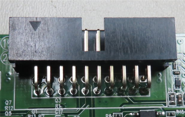
Here is a picture of the e-paper module's interface connector (box header).

Can you spot anything wrong with it?

At first glance everything looks fine but it's not.

A hint - Have a look where the Pin 1 indicator is on the box header and where it is on the PCB.


Pin 1 of the connector is the bottom left hand corner pad

Pin 1 of the PCB is the top right hand corner pad that is square in shape.


In other words, a top keyed right angled box header side has been used instead of a vertical box header.

Another mix up with orientation with box headers is when they are mounted on the opposite side of the PCB and if you're not careful end up in a real pickle.


This was a common problem with IBM PC floppy disk controllers and cables.

The makeshift solution was to cut and grind the unwanted key of the connector cable to enable it to be plugged in to match the wiring.

(Some box headers had enough flex to have the key forced in without the need to remove the key).

Another orientation protection method used was the use small rubber bungs and missing connector pins to be used as additional keys so they could not be connected the wrong way around.


It's not the first or last time you will encounter something like this and it's a really easy way to ruin something.

As a general rule when laying out PCBs make sure that Pin 1 is on the left hand bottom corner with the connector edge at the top because this will ensure that a top keyed right angled box header can be used.


http://katalog.we-online.de/em/datasheet/6120xx21721.pdf

Anonymous
  • DAB
    DAB over 8 years ago

    Good catch Monte.


    It amazes me how many companies come up with a good idea, but then screw up the implementation by violating accepted conventions.


    Hopefully the manufacturer will correct the problem soon.


    DAB

    • Cancel
    • Up 0 Down
    • Reply
    • More
    • Cancel
Element14

element14 is the first online community specifically for engineers. Connect with your peers and get expert answers to your questions.

  • Members
  • Learn
  • Technologies
  • Challenges & Projects
  • Products
  • Store
  • About Us
  • Feedback & Support
  • FAQs
  • Terms of Use
  • Privacy Policy
  • Legal and Copyright Notices
  • Sitemap
  • Cookies

An Avnet Company © 2022 Premier Farnell Limited. All Rights Reserved.

Premier Farnell Ltd, registered in England and Wales (no 00876412), registered office: Farnell House, Forge Lane, Leeds LS12 2NE.

ICP 备案号 10220084.

Follow element14

  • Facebook
  • Twitter
  • linkedin
  • YouTube