


Previously, we learned how to take care of the high frequency ringing using a primary side RC snubber across our switch, but there was still a voltage spike that, while for the test circuit is fine, can really get to dangerous levels if we were to use rectified mains as our Vin. To take care of that there are different ways of clamping Vds to acceptable levels, but I'll only be covering...
The Zener Clamp
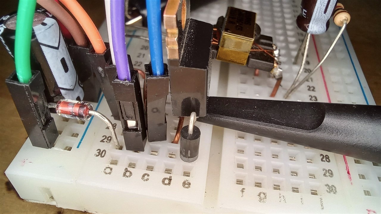
It consists of a pair of diodes in series, one of which is a fast recovery diode (in this particular case a schottky as they have virtually no reverse recovery time) and the other is a zener diode biased in reverse. Sure, nice, but how does this work?
For a more in-depth explanation of zener clamps, read TI's guide: Mitigating Procedure on Voltage Spike of Switching Node from Flyback Converter
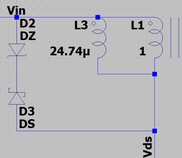
We saw when exploring the flyback cycle in DCM in the previous blog that Lm stores energy during the ON portion of the cycle, and releases it to the ideal transformer during the OFF portion, and this ideal transformer tansfers the energy to the secondary right away. To accomplish that, a voltage is induced at the secondary that goes as high as is required for the powers to balance on both sides of the transformer. This also happens the other way around, so a voltage is reflected from the secondary back into the primary, which is what causes the Vds waveform we've become familiar with so far. This reflected voltage (Vor) can be calculated like this for our ideal circuit:
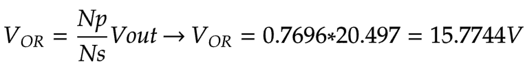
This voltage is measured from Vdrain to Vin during the OFF portion of the cycle. When the switch is ON, the voltage measured between those nodes would be -Vin since the ideal MOSFET's drain and source would be at the same ground potential, 0V.
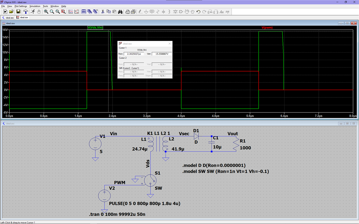
So if we have a maximum voltage of ~16V between those nodes, current will begin flowing across the clamp when the voltage reaches the forward voltage of our schottky plus the zener voltage of our zener, and remain at that level until Vor drops lower than that. In our ideal model, a zener clamp isn't of any use because there isn't a spike to suppress and this also limits the transfer of energy, as can be interpreted from the now droopy secondary current waveform:
But as the spike is generated from the inductive kick resulting from the leakage inductance, suppressing it won't affect the energy transfer, but will keep our MOSFET safe.
So, we see that if we use a clamp voltage lower than the ideal maximum Vor, we affect energy transfer. This means our clamp voltage must be between the spike's voltage and the ideal Vor. Another important consideration is the power dissipated by the zener, so this type of clamp can't be used in all cases, since the voltage spike might reach high enough voltage above the Vor plateau that the power rating needed would be impractical.
Let's figure out the best zener value for our converter through experimentation.
I have in my parts box 3 differently rated zener diodes: 12, 15, and 20V, and I'll be testing each of them without the previously calculated snubber, to see how they do on their own:
12V goes first:

This has taken care of the massive 36V spike we saw on the previous blog, and while the ringing is still there, it's nowhere near as bad as it was. Still, we see a considerable drop in voltage from almost 19V to almost 17V. This means 12V is definitely not the right voltage for our zener as we're now losing energy in the clamp that we wanted to transfer to the load.
Next, 15V:

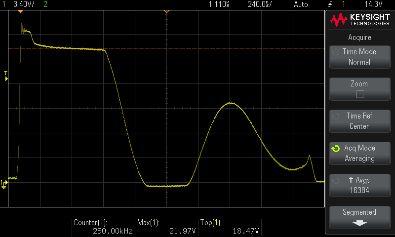
This voltage seemed oddly high, so I went to take a look at Vor:
Hmmm, that large spike still doesn't look right.
let's then take a look at the zener. I only have this TC1 component tester (see below) to measure the zener voltage, and while I wouldn't rely on it for actual quantitative measurements, it's good enough to get a general idea of what the values are.
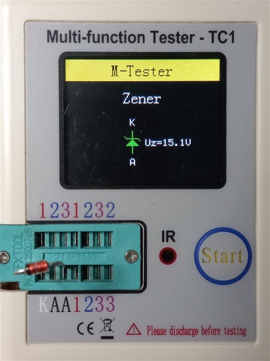
15.1V, not too bad, hmm!
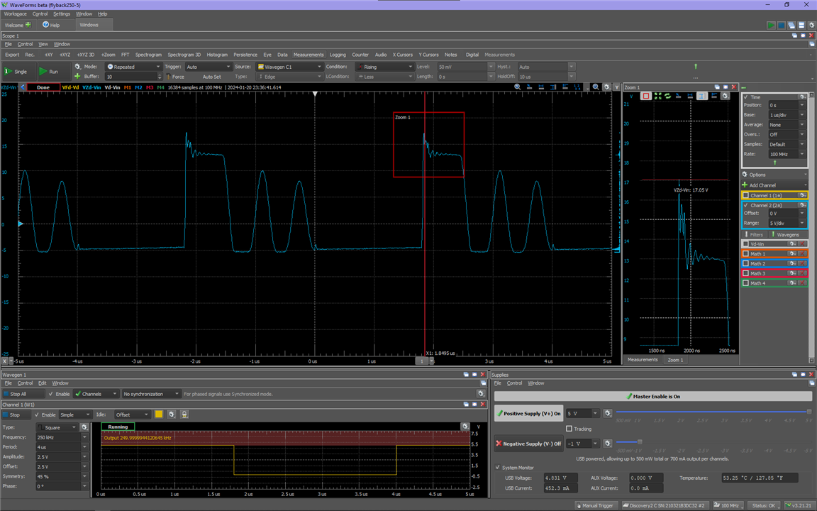
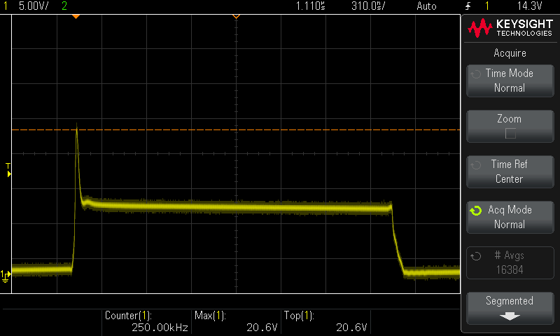
It seems the schottky is perhaps not being as fast as it should. I investigated for a while but couldn't determine the cause. Still, Vds as seen on the DSO reaches now a maximum of ~24V, and it plateaus at around 18.5V which is much closer to the original value, so that's great, not much of the useful energy is being wasted in the clamp. It seems this one would be a good fit to go with our snubber, but let's see how the 20V zener does:

Well, this is still doing something, not of much use to us since the snubber itself was bringing the spike down to about 24V already, and now with this showing a max of over 30V, I don't dare look at Vor with the Analog Discovery 2.
As the only reasonable option within my parts is the 15V zener, I'll be using that together with the snubber and see how they work together:

And here's what this looks like on the oscilloscope:
Quite the interesting result! While the clamp has indeed clamped Vds below the 24V spike we observed only with the snubber (at the end of the previous blog), it's really curious that some of the ringing is back. We can still see the slightly lower plateau at around 18.5V that we observed when using only the Zener, but that's acceptable, considering the limited options.
One thing we haven't looked at so far is...
The Output Voltage
So let's look at the voltages of the real world implementation, beginning from the snubbed and clamped circuit and going back to the minimal working implementation of it:
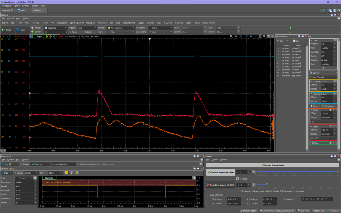
Channel 1, in yellow, shows us the input voltage.
Channel 2, in blue, shows us the output voltage.
We see an output voltage of about 16.7V, with a maximum of about 16.8V. Math3 (the red trace) zooms in on that, and we see a 100mV peak spike at the output, not too bad for our breadboard flyback converter. What is curious though, is what we see when zooming in on the input voltage (orange trace), 100mV max ripple riding on it, and its shape is very similar to that of the primary current we saw on the first blog. I'll expand on that input voltage noise in the next blog. For now, let's continue looking at the output voltage, this time, removing the zener clamp:

We observe a minor increase in output voltage as well as a slight change in the output ripple shape and its amplitude has gone up by almost a third.
Now let's see what happens when the snubber is also removed:

Well, that's not good at all!
This shows us another good reason to use snubber and clamp circuits in our flyback converters. Not only do they keep the MOSFET safe, they also help clean our output voltage, at a very minor cost. The output voltage drops by less than half a volt when both snubber and clamp are present, but it is also significantly cleaner, meaning it will inject considerably less noise both into the device we want to power and back into the DC source it's feeding from.
Pushing the boundary between operating modes
With the basics of how to design a flyback converter out of the way, it's time to see how this crudely constructed converter can continuously conduct current (ha! try saying that one out loud three times in a row)
First a quick look at the CCM voltage equation :
For more information about CCM operation, I recommend watching this video from katkimshow on Flyback Converter Operation and Voltage Equation from the Introduction to Power Electronics video series.
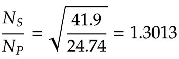
We consider the turns ratio as seen from the secondary, so in our case it would be:
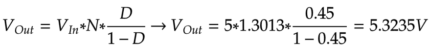
then
A quick simulation to check:
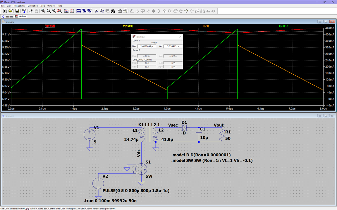
Close enough!
You see, the only change I made was to change the load from 1000 ohms to 50 ohms. This tells us that the mode of operation does not depend on the topology at all but the parameters, such as the output load, input voltage and duty cycle. In this case, only changing one of those parameters was enough to enter CCM in a circuit that we previously considered to be DCM only!
Moving onto the real life circuit, I'm now powering it with this external supply (which actually measures at 5.5V) since the AD2's supply keeps shutting off due to overcurrent (when going into CCM):
This is what Vds looks like, no snubber, no clamp:

Just what we expected, same 36V spike, same ringing frequency, just no lower frequency ringing as that behaviour is unique to DCM
And the input and output voltages:

Just as noisy as the barebones voltage in DCM operation!
And here's what it looks like when using both snubber and clamp:
And here's Vds:
All a lot more reasonable now, that spike is still clamped with a 15V zener, so that's to be expected, but still a lot more reasonable than the barebones 36V spike. If designing for CCM, you need to adjust the clamp value as well.
And finally, a simulation for good measure, using snubber and clamp with realistic components in which we can observe the current waveforms and see that they really don't reach 0 before the opposite winding begins to conduct:

We see Vout is lower than what we calculated and saw in the ideal simulation, and this is because that equation doesn't consider any losses in the circuit, but it still gives us a ballpark for what we should expect of our circuit when designing a converter.
From this load changing experiment we learned a few things:
- When everything else remains the same, except for the load, the converter operation can change, going from DCM to CCM and viceversa.
- This change in operation mode also means there will be a change in voltage, explained by the two different output voltage equations between CCM and DCM.
- Even if the load change is not significant enough to change the operation mode, the output voltage will change. To compensate for this, a control system with feedback is necessary.
- This showcased the buck/boost operation of flyback converters. Everything else being the same, we saw how the voltage went from over 3 times that of the supply to a little below the supply. Changing other parameters, for example the duty cycle can also result in voltages higher or lower than the supply.
- In this experiment the duty cycle remained constant at 45%, so this also shows that the duty cycle alone isn't what determines if the converter will behave as a step-up or step-down converter.
Moving Forward
In the next few blogs, I'll explore:
- Common mode filters
- The math is basically over. We'll take a quick look at calculating common mode filters, comparing a calculated filter with a filter built around available parts, and what else we can do to de-noise our supply rails.
- Part selection for a specific application.
- This will include a more in-depth look at the kit, and I'll select the appropriate transformer to use for my application.
- Bringing that application to life.
- I'll quickly go through the design process of the supply for my application. I'll try using a pre-made controller adapted to that design, and we'll see how well that goes.
Even if this is just the middle point for me in this contest, it feels as if the hardest part is over. If you also read the previous two blogs, designing a flyback converter should bring you not much trouble. I hope I was able to provide you with fun to read, easy to understand valuable content, and I'd love to see you bringing flyback supplies to life.
The next blogs will include more hands-on content, but of course, I'll sneak in a few more simulations.
As usual, all feedback is welcome.
Thank you! 


