

When several months ago, during a forum discussion what would be needed in the challenger's kit for SPE design challenge, kmikemoo suggested that LTC9111 Powered Device chip would be interesting.
In that time I have thought that it would be too time consuming to make use of it, but it the meantime, as a byproduct of some research, I have asked ADI for samples of both LTC9111 and LTC4296 (matching Power Sourcing Equipment controller) and they generously sent me them.
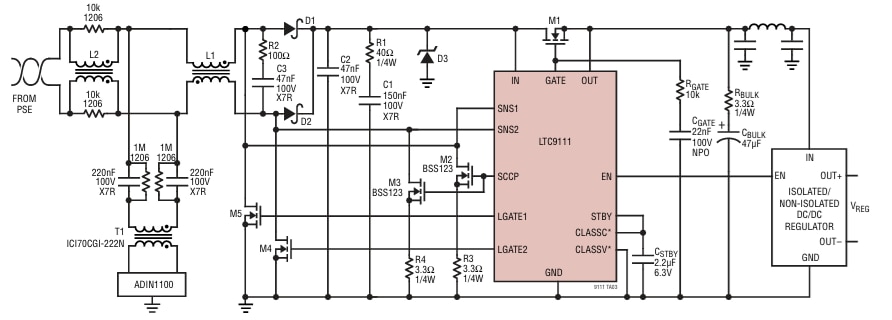
LTC9111 datasheet specifies typical schematics as below:
and the chip itself is operating according to the PD state machine like below:
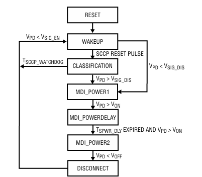
which involves PSE-PD discovery process, allowing for proper PD classification and management.
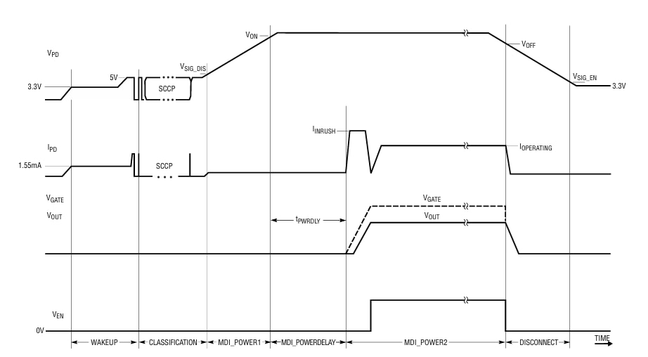
During the discovery, PSE raises line voltage (with current limit enforced) to about 5V, then initiates communication.
When voltage is about 5V, classification can begin. It is done using one-wire SCCP protocol, which involves pulling down the power line at the transmitter side for predefined time.
LTC9111 is powered using Cstby capacitor during power down pulses and is using M2/M3 MOSFET pair to pull down power line by it's own (as the system is designed to be polarity-agnostic, symmetric design is used).
Communication is started by the PSE which sends reset pulse and PD answers with presence pulse. Then, PD transmits it's power class and, when accepted, PSE raises line voltage to the negotiated value. Then, PD opens M1 MOSFET and raises ENABLE signal, starting providing power to the load.
When voltage on the line drops, ENABLE signal is lowered and M1 closed.
Six power classes are defined (and can be configured using two three-state pins of LTC9111), three for supply voltage up to 30V and three for voltage up to 58V
| Class | max power [W] | PD voltage [V] |
| 10 | 1.23 | 14-30 |
| 11 | 3.2 | 14-30 |
| 12 | 8.4 | 14-30 |
| 13 | 7.7 | 35-58 |
| 14 | 20 | 35-58 |
| 15 | 52 | 35-58 |
As the solution is expected to work over long data lines, which may involve significant voltage drop - and, as we have previously discovered and confirmed in the requirements - signal polarity needs to be corrected if needed, low-loss rectifier is built using D1 and D2 Schottky diodes and M4 and M5 MOSFETs (from which one is activated when voltage polarity is sensed using SNS1 and SNS2 inputs to further reduce voltage drop). Before M4/M5 activation, current flows through their reverse parasitic diodes, effectively forming traditional Graetz bridge.
This solution is very advanced, but for the basic usage can be simplified: M4/M5 can be replaced with another set of Schottky diodes and some snubbing circuits can be (at least initially) omitted, leading to the circuit like below:
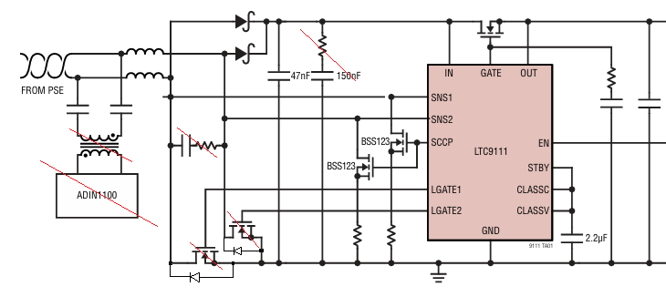
and PCB like below
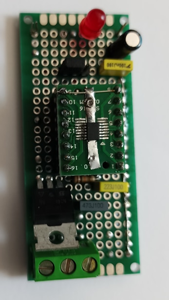
as can be seen, chip installation is rather unusual, but it is caused by the fact that exposed pad at the bottom is the one and only GND contact (chip is housed in MSOP-12 package but has 13 active contacts), and MSOP-DIP adapter PCB (unlike - for example - QFN adapters) usually lack additional trace below the chip.
So, MSOP adapter was modified by placing adhesive copper tape at the center, then secured by two rivets in case when the glue didn't survive soldering and it worked - almost. When hot air soldered, tape glue expanded, raising the chip above the PCB, which required additional work to correct.
Next time I will try to remove adhesive from the tape and fix it using proper glue - but I am unsure what type of glue should be used? Maybe some cyanoacrylate glue would work? Or maybe something better is needed?

