First and foremost, a massive thank you to the incredible team at the Element14 Community and our sponsor, TDK. I was absolutely thrilled to be selected as one of the nine sponsored challengers for the In Reach! Ultrasonic Sensor Sensing Challenge, and it was a fantastic feeling to receive the official challenger's kit. The support from this community is what makes these creative endeavors possible, and I'm honored to be a part of it.
In this first blog, we'll take a detailed look at the TDK Demo Kit and I'll be sharing my unboxing experience and my initial thoughts on the build quality and design of the USSM1.0 PLUS-FS sensors along with it's evaluation board.
2. The Unboxing
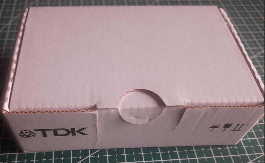
There's a special kind of excitement that comes with opening a box of brand-new, high-quality hardware and TDK did not disappoint.
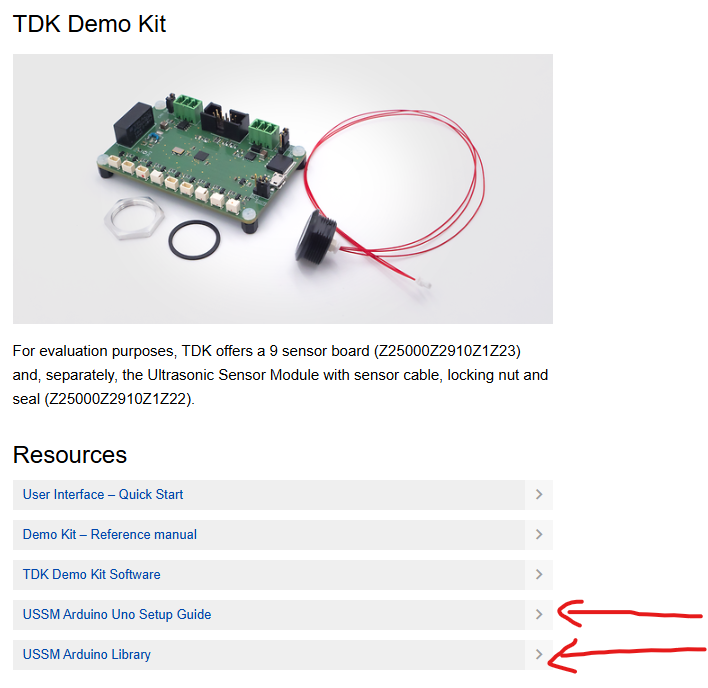
The kit arrived securely packaged, with each component neatly nestled in its own protective packaging. TDK's focus on a smooth start is also evident. Right on the packaging, helpful QR codes are provided, instantly linking to the datasheets and guides needed to dive right in.
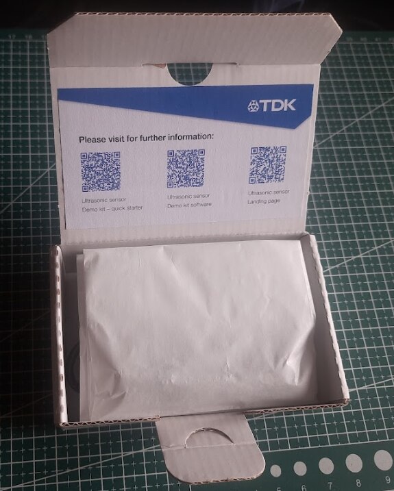
Before I even got to the hardware, I was immediately impressed by the packaging. It's clear TDK has prioritized sustainability, using eco-friendly and biodegradable materials for the main insert. The only plastic in sight was the essential anti-static bag protecting the demo board—a necessary measure. In an industry often dominated by single-use plastics, this thoughtful approach is something to be applauded!
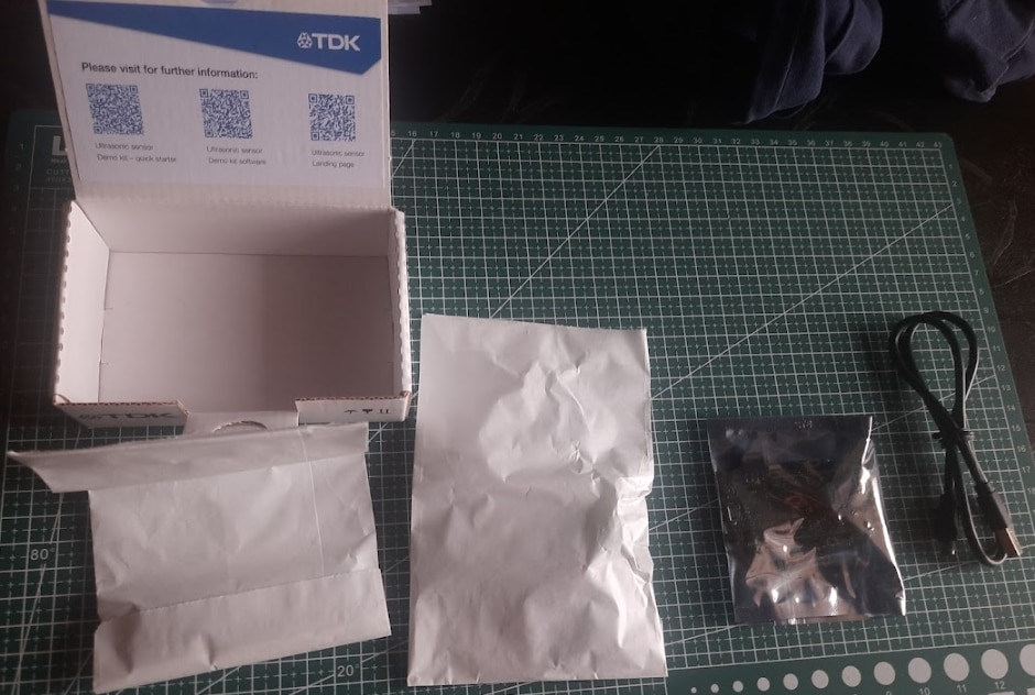
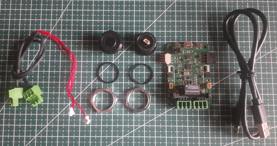
Inside the box, I found 2x sensor connection cables, 2x USSM1.0 PLUS-FS ultrasonic sensor along with it's locking nut and rubber gasket, 1x TDK USSM Demo Board and 1x Micro-B to USB-A cable.
3. Hardware Deep Dive
Now that everything is out of the box, let's go beyond the surface and dive into the hardware and it's specifications.
3.1 TDK USSM1.0 PLUS-FS Ultrasonic Sensor
The core component of this challenge is the USSM1.0 PLUS-FS ultrasonic sensor module. It is a self-contained piezo-based sensor unit with an integrated Application-Specific Integrated Circuit (ASIC), the E524.33 (IC's document is linked in the Resources section of the sensor's product page but not specified explicitly in the documentation of the sensor) that handles the ultrasonic signal processing internally.
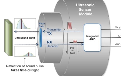
The principle of operation is Time-of-Flight (ToF), which is a method for measuring distance by precisely timing the journey of a wave. The process is as follows:
- Transmission: The sensor emits a short, high-frequency burst of sound (an ultrasonic pulse of frequency of 74.5 KHz) into the air.
- Propagation: This sound wave travels outwards from the sensor at the speed of sound (c).
- Reflection: When the wave encounters an object, it reflects off the surface, creating an echo that travels back towards the sensor.
- Reception: The sensor's piezoelectric element detects the faint returning echo.
- Calculation: The integrated ASIC measures the total elapsed time (T) from the moment the pulse was transmitted to the moment the echo was received.
Because the sound wave traveled to the object and back, the one-way distance (L) is half of the total distance traveled.
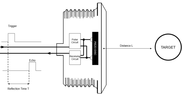
This relationship is defined by the fundamental ToF formula:
L = (c * T) / 2
The E524.33 is responsible for managing this entire sequence—from generating the driver signal for the burst to amplifying and filtering the received echo and performing the time measurement. This high level of integration simplifies the end application significantly, as the module provides reliable data without requiring complex external signal conditioning circuitry (E524.33's signal processing pipeline will be explored in further upcoming blogs).
According to the technical datasheet, the sensor exhibits robust performance characteristics.
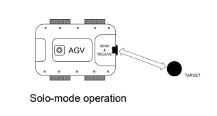
In its standard "solo mode," where a single sensor handles both transmission and reception, it features an operating range from 18 cm to 5 m.
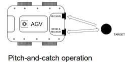
And the module also supports a "pitch-and-catch mode," which utilizes two sensors (one as emitter, one as receiver) to achieve a significantly reduced minimum detection distance of just 4 cm.
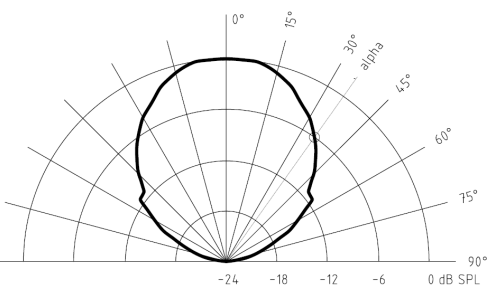
The sensor is capable of a fast sample rate of up to 50 samples per second ( i.e 20 ms update interval), fast enough for real-time tracking and dynamic object detection and has a symmetric directivity of ±35°, providing a wide field of view for object detection.
From an electrical standpoint, the module is designed for easy integration, requiring only a single power supply ranging from 8 V to 18 V (typically 12 V) to drive all its internal electronics. The current consumption is a nominal 5.5 mA, making it suitable for power-conscious applications.
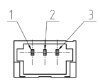
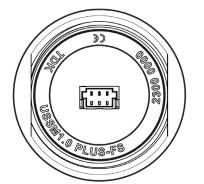
Interfacing is handled via a simple 3-pin connector (present at the rear of the sensor) which provides power (1. VSUP), ground (2. GND), and a single proprietary bidirectional IO line(3. IO) for all digital communication between the sensor and a host.
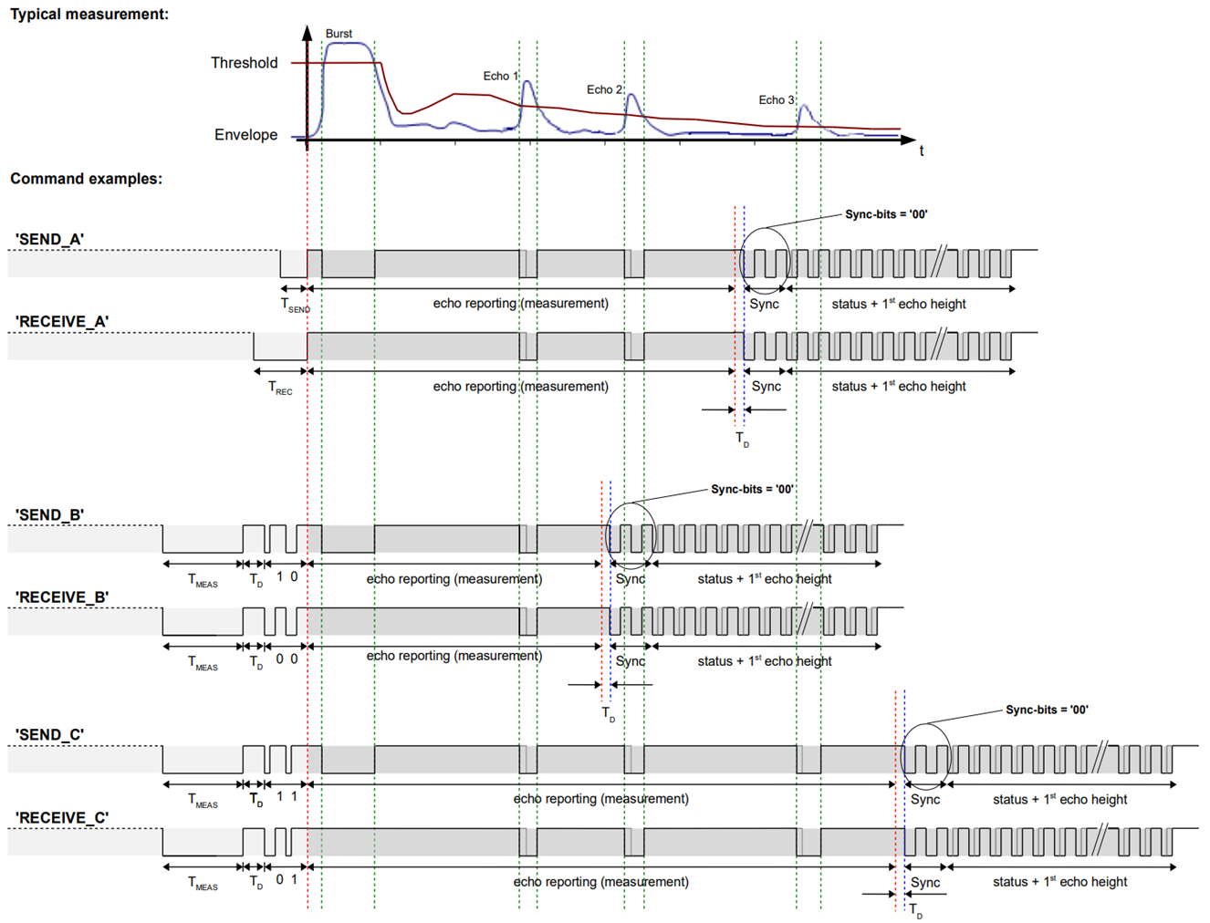
The standout feature here is the single-wire IO interface. Rather than separate trigger and echo pins or a complex serial protocol, employs a proprietary PWM-based communication scheme where the duration of low pulses encodes logical '0's and '1's. This bidirectional protocol supports a comprehensive command set, allowing deep customization of sensor behavior—detection thresholds, sampling modes, filtering parameters, and more—all negotiated over a single wire.
While this proprietary protocol means you can't simply drop the sensor into an Arduino sketch without additional library support, it's a clever trade-off that minimizes pin count and simplifies routing in complex systems. The TDK evaluation board handles protocol translation, but understanding the underlying PWM encoding will be crucial for custom integrations (another topic I'll dissect in future posts).
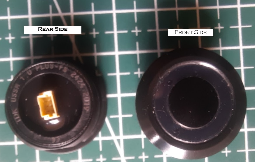
The E524.33 ASIC and supporting circuitry are potted in black epoxy resin, leaving only the 3-pin connector exposed. This encapsulation provides excellent moisture resistance, chemical protection, and mechanical durability—critical for the outdoor, harsh-environment applications the sensor is marketed toward.
Upon closer inspection, the professional finish of the sensor extends to its clear and comprehensive labeling. Each sensor is permanently marked with key information, which is essential for traceability and identification in a development or production environment.
These markings include:
- TDK: Manufacturer
- USSM1.0 PLUS-FS: Product and variant identification code.
- YYCW XXXX: A unique serial number which also encodes the year and week of production.
- CE mark: Indicates conformity with health, safety, and environmental protection standards for products sold within the European Economic Area (EEA).
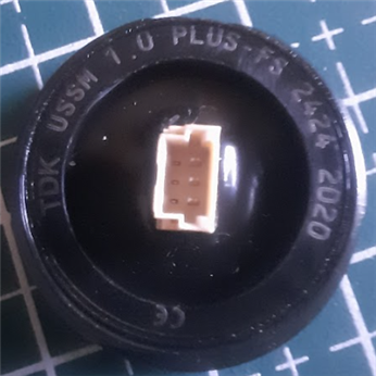
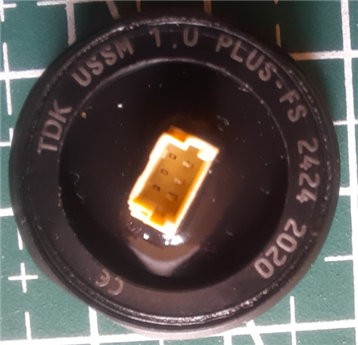
My two sensors carry serial numbers 2019 and 2020, both manufactured in calendar week 24 of 2024 (2424 marking). This level of traceability is uncommon in maker-space components but essential for quality control, warranty claims, and compliance documentation in commercial deployments.
3.2 Sensor Connection Cables
While often overlooked, the quality of the interconnects is critical for a reliable system. The kit includes two dedicated sensor connection cables that serve as the vital link between the TDK USSM1.0 PLUS-FS sensors and the USSM Demo Board. The build quality of the cables is excellent. The wiring is appropriately gauged for delivering power and carrying the high-speed data signals without degradation. The length of the cables is generous, providing ample flexibility for benchtop prototyping and for positioning the sensors at a reasonable distance from the evaluation board.
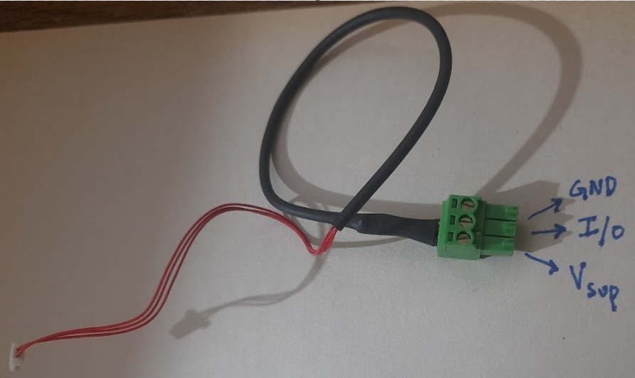
Each cable is terminated with two distinct connectors:
- Sensor End: A compact, white 3-pin female connector designed to mate perfectly with the integrated socket on the rear of the USSM sensor.
- Board End: A slightly larger, green 3-pin female 3.5mm pluggable screw terminal that plugs directly into the corresponding male headers on the TDK evaluation board.
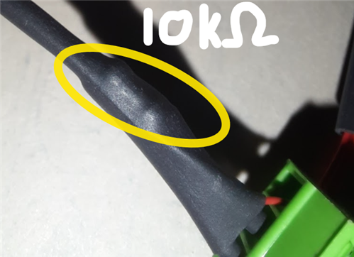
Note : There's a 10K Ohms pull-up resistor hidden within the cable between the Vsup and the IO pins.
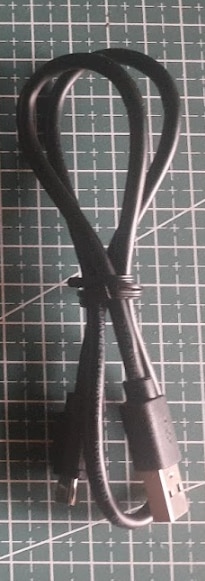
3.3 Micro USB-B to USB-A Cable
A stable and reliable connection to the host computer is fundamental for development. The kit includes a high-quality Micro-B to USB-A cable that serves this dual purpose, providing both power to the entire evaluation board and the data channel for programming and monitoring.
Upon inspection, the cable sheath is marked with its full technical specification: "USB SHIELDED HIGH SPEED CABLE 2.0 REVISION 28AWG/1P + 28AWG/2C". This string is not just for identification; it is a concise summary of the cable's construction and certifies its performance capabilities.
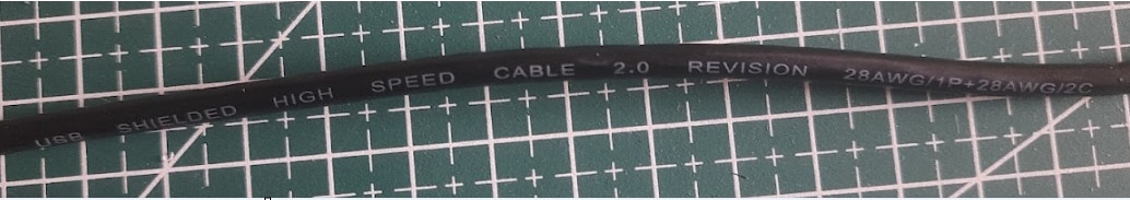
Let's dissect this specification
- USB HIGH SPEED CABLE 2.0 REVISION: This confirms the cable is fully compliant with the USB 2.0 standard, designed to support "High Speed" data rates of up to 480 Mbit/s. This ensures fast and efficient communication for programming the board and for real-time data streaming from the sensor without bottlenecks.
- SHIELDED: This is a critical feature for ensuring signal integrity. The internal wires are wrapped in a metallic shield (a foil or braid) that protects the data and power lines from external electromagnetic interference (EMI). In a project environment that will include motors and other sources of electrical noise, this shielding is essential for preventing data corruption and ensuring stable operation.
- 28AWG/1P (1 Pair): This indicates the cable contains one twisted pair of 28AWG (American Wire Gauge) wires. The USB 2.0 standard requires the data lines (D+ and D-) to be twisted together. This design cancels out crosstalk and external noise, which is fundamental for maintaining error-free, high-speed data transmission.
- + 28AWG/2C (2 Conductors): This refers to the two additional single conductors of 28AWG wire within the cable. These are dedicated to power delivery: one for the +5V supply and one for Ground (GND). The 28AWG thickness is standard and appropriately sized to deliver the necessary current to power the USSM Demo Board and its connected sensors.
3.4 TDK USSM Sensor Demo Board
The TDK USSM Demo Board is a comprehensive development and evaluation platform engineered specifically for the USSM series of ultrasonic sensors. It serves as a hardware abstraction layer, providing the necessary power, communication, and processing capabilities to interface the sensors with a host PC.
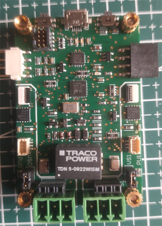
Top Side View
Bottom Side View
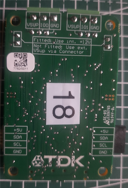
The first impression of the board is one of high-quality manufacturing. The 2-layer PCB construction feels robust and well-manufactured, with a clean layout that suggests thoughtful design consideration. Component placement follows a logical hierarchy, avoiding the cramped, chaotic arrangement often seen in budget development boards. The soldering quality is exceptional—clean joints, consistent fillet formation, and no cold solder bridges or flux residue, indicating precision manufacturing processes.
However, the board isn't without its usability quirks. The most glaring omission is the lack of silkscreen labeling for key components. While this minimalist aesthetic might appeal to experienced developers, it creates an unnecessary barrier for newcomers. The buttons, in particular, present a guessing game—without clear markings indicating which is BOOT and which is RESET needing to reference the documentation. This becomes especially frustrating during rapid prototyping when quick resets are needed.
Here's the image labelling the connectors on the board as provided in the documentation :
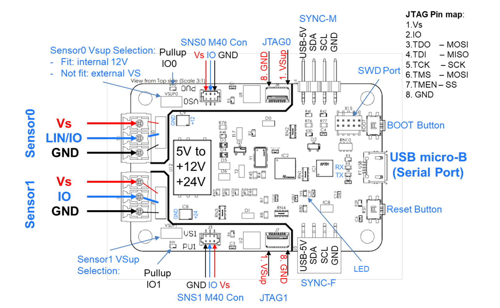
Now let's look into other functional IC's on board,
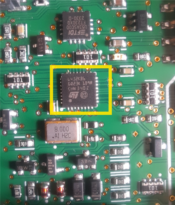
The board is populated with an STM32L432KBU6 MCU, a high-performance, ultra-low-power microcontroller from STMicroelectronics based on the Arm Cortex-M4 core, equipped with an FPU and DSP instructions for efficient data processing. The firmware leverages its on-chip peripherals, including Timers (in Input Capture mode for precise signal decoding), UART (for communication between the sensors through LIN Transceivers), and GPIOs.
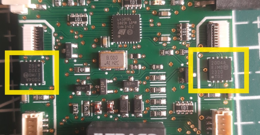
A critical component of the demo board's robust design is the use of a Microchip MCP2004A LIN transceiver for each sensor port. While the USSM sensor communicates via a proprietary single-wire protocol, the MCP2004A is employed as an exceptionally effective and hardened physical layer to bridge this protocol with the MCU's logic-level I/O UART.
- Component and Functionality: The MCP2004A is a LIN Bus-compliant transceiver that serves as a bidirectional, high-voltage I/O buffer. Its primary role in this application is to provide robust voltage level shifting and a protected physical interface for the sensor's single IO line.
- Voltage Level Shifting: The transceiver expertly translates signals between two different voltage domains. It converts the MCU's 3.3V logic-level signals from a UART TX pin into the higher-voltage signals on the sensor's IO line, which is pulled up to the VSUP rail (typically +12V). In the reverse direction, it detects the high-voltage signaling from the sensor on the bus and converts it back down to a clean 3.3V logic-level signal on its RXD pin, which is then fed to the MCU.
- Signal Integrity and Protection: As an automotive-grade component, the MCP2004A provides significant built-in protection. It features high ESD protection on the bus pin, safeguarding the more sensitive MCU from electrical transients. It also has a controlled slew rate on its output driver, which is crucial for minimizing electromagnetic interference (EMI)—an important consideration in a system with potential noise sources like motors.
- Signal Path: To send a command, the STM32's UART TX pin drives the MCP2004A's TXD input. The transceiver, in turn, drives the main LBUS pin (connected to the sensor's IO line) to the appropriate voltage level. When the sensor responds by pulling its IO line low, the MCP2004A detects this state change on the LBUS pin and mirrors it on its RXD output pin. This 3.3V signal is then precisely measured by the STM32's timer peripheral to decode the incoming data.
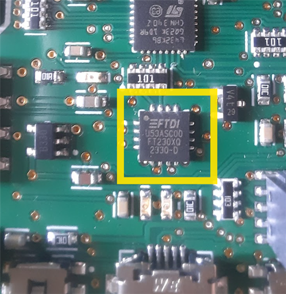
Host communication is managed by a dedicated FTDI FT230XQ USB-to-UART bridge IC, ensuring maximum driver stability and compatibility by presenting a standard virtual COM port to the host PC.
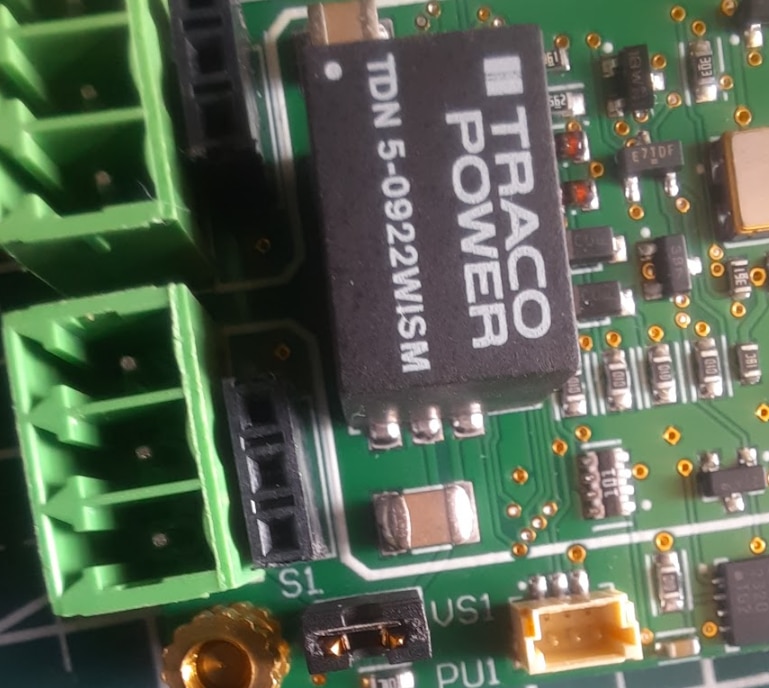
The board's power architecture is fully self-contained, deriving all power from the 5V USB VBUS. The generation of the higher voltages required by the sensors and their interface circuitry is handled by a single, highly integrated component: a TRACO POWER TDN 5-0922WISM DC-DC converter module. The selection of a complete module rather than a discrete controller IC is a significant design choice that prioritizes reliability, noise immunity, and simplification of the board layout.
A key specification of this component is its I/O isolation, rated at 1.6 kVDC, which electrically separates the input ground (tied to the host PC) from the output ground used by the sensor circuitry. This isolation is critical for preventing ground loops and protecting the host system from potential electrical faults or transients on the sensor side.
The module is designed for a nominal 5V input, making it perfectly suited for direct operation from the USB VBUS. A defining feature is its dual-output capability; it simultaneously generates two independent, regulated voltages from the single input.
The primary +12V rail serves as the operational supply (VSUP) for the USSM sensors and provides the necessary voltage for the MCP2004A LIN transceivers.
The secondary +24V rail is dedicated to a specific, high-voltage function: the programming of the sensor's internal EEPROM.
Furthermore, the module incorporates a Remote On/Off pin, which is connected directly to a GPIO of the STM32 microcontroller. This provides the firmware with programmatic control to enable or disable the entire high-voltage power stage, allowing for advanced power management or, more critically, the ability to perform a hard power-cycle reset of the sensors by toggling their VSUP supply.
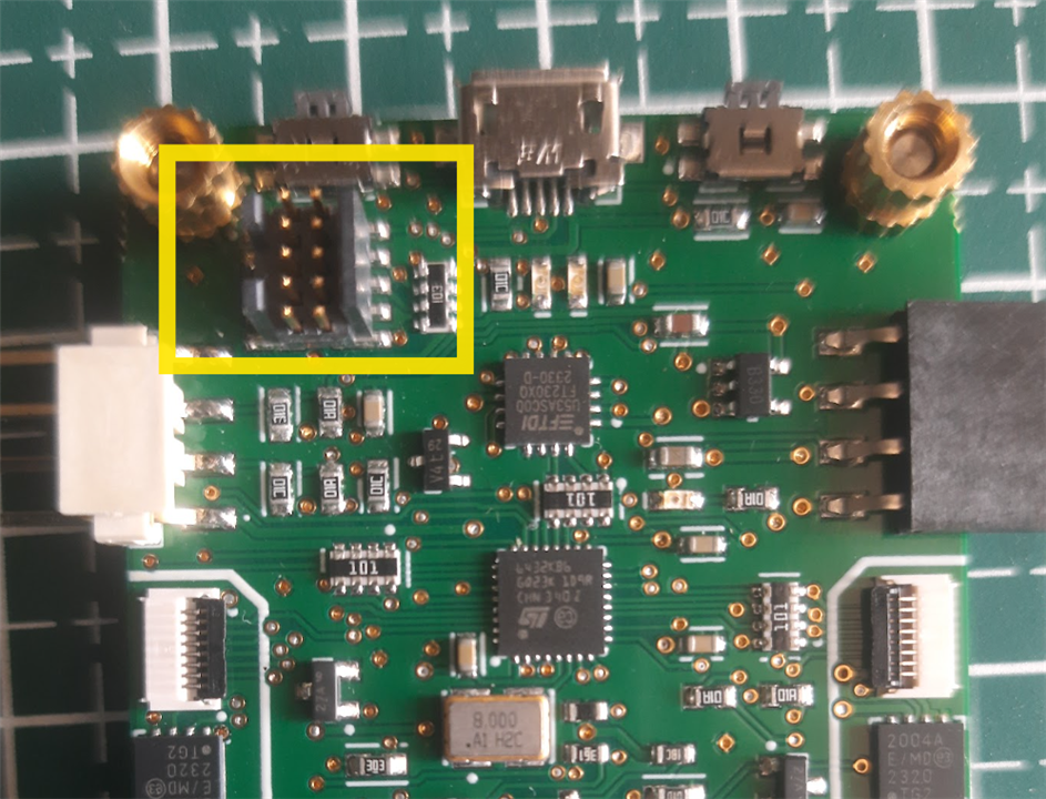
The board also includes standard SWD (Serial Wire Debug) access for in-circuit programming and debugging, along with RESET and BOOT buttons for manual MCU control during firmware development.
Now that I have a comprehensive understanding of the hardware's capabilities, the next phase is to bring the system online. In my upcoming post, I will connect the USSM sensors to the evaluation board and power up the hardware for the first time. From there, I'll conduct a detailed walkthrough of the TDK demo software, exploring its GUI and configuring the various sensor parameters to capture my first live distance measurements.