element14 Community
element14 Community
    Register Log In
  • Site
  • Search
  • Log In Register
  • About Us
  • Community Hub
    Community Hub
    • What's New on element14
    • Feedback and Support
    • Benefits of Membership
    • Personal Blogs
    • Members Area
    • Achievement Levels
  • Learn
    Learn
    • Ask an Expert
    • eBooks
    • element14 presents
    • Learning Center
    • Tech Spotlight
    • STEM Academy
    • Webinars, Training and Events
    • Learning Groups
  • Technologies
    Technologies
    • 3D Printing
    • FPGA
    • Industrial Automation
    • Internet of Things
    • Power & Energy
    • Sensors
    • Technology Groups
  • Challenges & Projects
    Challenges & Projects
    • Design Challenges
    • element14 presents Projects
    • Project14
    • Arduino Projects
    • Raspberry Pi Projects
    • Project Groups
  • Products
    Products
    • Arduino
    • Avnet Boards Community
    • Dev Tools
    • Manufacturers
    • Multicomp Pro
    • Product Groups
    • Raspberry Pi
    • RoadTests & Reviews
  • Store
    Store
    • Visit Your Store
    • Choose another store...
      • Europe
      •  Austria (German)
      •  Belgium (Dutch, French)
      •  Bulgaria (Bulgarian)
      •  Czech Republic (Czech)
      •  Denmark (Danish)
      •  Estonia (Estonian)
      •  Finland (Finnish)
      •  France (French)
      •  Germany (German)
      •  Hungary (Hungarian)
      •  Ireland
      •  Israel
      •  Italy (Italian)
      •  Latvia (Latvian)
      •  
      •  Lithuania (Lithuanian)
      •  Netherlands (Dutch)
      •  Norway (Norwegian)
      •  Poland (Polish)
      •  Portugal (Portuguese)
      •  Romania (Romanian)
      •  Russia (Russian)
      •  Slovakia (Slovak)
      •  Slovenia (Slovenian)
      •  Spain (Spanish)
      •  Sweden (Swedish)
      •  Switzerland(German, French)
      •  Turkey (Turkish)
      •  United Kingdom
      • Asia Pacific
      •  Australia
      •  China
      •  Hong Kong
      •  India
      •  Korea (Korean)
      •  Malaysia
      •  New Zealand
      •  Philippines
      •  Singapore
      •  Taiwan
      •  Thailand (Thai)
      • Americas
      •  Brazil (Portuguese)
      •  Canada
      •  Mexico (Spanish)
      •  United States
      Can't find the country/region you're looking for? Visit our export site or find a local distributor.
  • Translate
  • Profile
  • Settings
In the Air Design Challenge
  • Challenges & Projects
  • Design Challenges
  • In the Air Design Challenge
  • More
  • Cancel
In the Air Design Challenge
Blog Carbon Footprint Monitoring - Hardware Design
  • Blog
  • Forum
  • Documents
  • Polls
  • Files
  • Events
  • Mentions
  • Sub-Groups
  • Tags
  • More
  • Cancel
  • New
  • Share
  • More
  • Cancel
Group Actions
  • Group RSS
  • More
  • Cancel
Engagement
  • Author Author: xever
  • Date Created: 16 Dec 2014 8:43 AM Date Created
  • Views 358 views
  • Likes 2 likes
  • Comments 0 comments
  • iot_footprint
  • in_the_air_design_challenge_2014
  • in_the_air
Related
Recommended

Carbon Footprint Monitoring - Hardware Design

xever
xever
16 Dec 2014

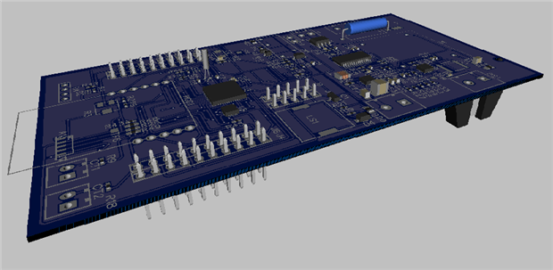
Over the past few days, I have been contemplating about the hardware for this particular project and ended up with a PCB design as rendered below.


image


Initial Thoughts


How I came into this design was a result of a thought process that attempted to answer the following questions:

1.  How many different sensor nodes are there in the system

2.  What are the similarities/differences between each node

3.  How can each node feature requirements be normalised so as to deliver a minimum viable design

4.  What could be done in the design to have a cost effective PCB run

5.  What design considerations can be put in the board design for ease of debugging and profiling

6.  Which components to be used? Considering project requirement vs design challenge recommendation as well as component availability vs component cost.


Based from the above guideline, I looked back at my proposed system and reviewed the different sensor nodes and found that there are indeed similarities and that these can be grouped together.  As an example, both the indoor and outdoor sensors are particularly identical, except for their power supply.  Aside from the outdoor sensor being powered through solar energy, it has an additional current sensor which the indoor version does not have, instead the indoor sensor has a buzzer. You can refresh yourself by revisiting this post.


The Smart Plug and Smart Switches are basically 'electronically' identical and the variation will be on the mechanical (enclosure) design.  Comparing the smart plug, smart switch, indoor sensor, and outdoor sensor, again there are similarities among them.  They all use the Texas Instruments' CC3200 module, and that is another common aspect being brought into consideration.


Among the different sensor nodes, the emission sensor is quite unique among them.  It uses the MSP430FR5969 MCU instead of the CC3200, at the same time uses Bluetooth Smart instead of WiFi.  So at this stage, I thought of designing two PCB boards.


CC3200-based Sensor Node


And so I started creating a schematic for a CC32000-based sensor node... and upon completing the schematics which was largely based on the Launchpad XL design, I then started to shop for electronic components... and... found that the price for CC3200 MCU's at element14 costs NZ$33.43 while the LaunchpadXL costs $NZ44.96.  So I started pondering on the thought that if I would continue to roll my own board, the BOM cost would be more than the price of a Launchpad PLUS the million risks in getting it right especially around the antenna section of the design.  Thus, it was logical to purchase a couple more or so Launchpads and instead take the booster pack approach.


Booster Pack Design


I kept the schematics and moved on to design a booster pack instead that would fit both (CC3200 and MSP430FR45969) Launchpads.  Everything is going quite on track until I realised that there aren't enough available IO's on the MSP430FR5969-EXP board.  Another revision of the design was inevitable, and this time, I have to incorporate an MSP430FR5969 chipset into the booster pack design.  And that's how the board came about.


Board Sections


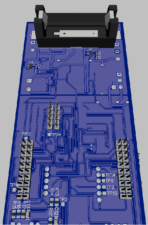
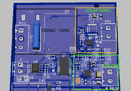
Below are renders of the Top (image on the left) and Bottom (image on the right) assembly.  I did not bother on the missing 3D models, the render should be enough to explain the different sections and main components of the board.

imageimage


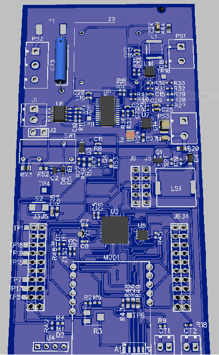
The top section is where the power supply(s) are laid.  See below.

image

Battery is placed in the bottom assembly.


The idea here is to only populate the section relevant to the sensor node.  Thus saving a bit on PCB manufacturing costs.

U3 in the center of the lower part of the board is the MSP430FR5969, which will be populated for the emission sensor node. 

MOD1 is placeholder for the Bluetooth Smart (nRF8001) module.


This is all for this week's post.  I will provide more information about the board when they arrive.

Attachments:
imageSchematic - InTheAir.pdf
  • Sign in to reply
element14 Community

element14 is the first online community specifically for engineers. Connect with your peers and get expert answers to your questions.

  • Members
  • Learn
  • Technologies
  • Challenges & Projects
  • Products
  • Store
  • About Us
  • Feedback & Support
  • FAQs
  • Terms of Use
  • Privacy Policy
  • Legal and Copyright Notices
  • Sitemap
  • Cookies

An Avnet Company © 2025 Premier Farnell Limited. All Rights Reserved.

Premier Farnell Ltd, registered in England and Wales (no 00876412), registered office: Farnell House, Forge Lane, Leeds LS12 2NE.

ICP 备案号 10220084.

Follow element14

  • X
  • Facebook
  • linkedin
  • YouTube