element14 Community
element14 Community
    Register Log In
  • Site
  • Search
  • Log In Register
  • Community Hub
    Community Hub
    • What's New on element14
    • Feedback and Support
    • Benefits of Membership
    • Personal Blogs
    • Members Area
    • Achievement Levels
  • Learn
    Learn
    • Ask an Expert
    • eBooks
    • element14 presents
    • Learning Center
    • Tech Spotlight
    • STEM Academy
    • Webinars, Training and Events
    • Learning Groups
  • Technologies
    Technologies
    • 3D Printing
    • FPGA
    • Industrial Automation
    • Internet of Things
    • Power & Energy
    • Sensors
    • Technology Groups
  • Challenges & Projects
    Challenges & Projects
    • Design Challenges
    • element14 presents Projects
    • Project14
    • Arduino Projects
    • Raspberry Pi Projects
    • Project Groups
  • Products
    Products
    • Arduino
    • Avnet & Tria Boards Community
    • Dev Tools
    • Manufacturers
    • Multicomp Pro
    • Product Groups
    • Raspberry Pi
    • RoadTests & Reviews
  • About Us
  • Store
    Store
    • Visit Your Store
    • Choose another store...
      • Europe
      •  Austria (German)
      •  Belgium (Dutch, French)
      •  Bulgaria (Bulgarian)
      •  Czech Republic (Czech)
      •  Denmark (Danish)
      •  Estonia (Estonian)
      •  Finland (Finnish)
      •  France (French)
      •  Germany (German)
      •  Hungary (Hungarian)
      •  Ireland
      •  Israel
      •  Italy (Italian)
      •  Latvia (Latvian)
      •  
      •  Lithuania (Lithuanian)
      •  Netherlands (Dutch)
      •  Norway (Norwegian)
      •  Poland (Polish)
      •  Portugal (Portuguese)
      •  Romania (Romanian)
      •  Russia (Russian)
      •  Slovakia (Slovak)
      •  Slovenia (Slovenian)
      •  Spain (Spanish)
      •  Sweden (Swedish)
      •  Switzerland(German, French)
      •  Turkey (Turkish)
      •  United Kingdom
      • Asia Pacific
      •  Australia
      •  China
      •  Hong Kong
      •  India
      •  Korea (Korean)
      •  Malaysia
      •  New Zealand
      •  Philippines
      •  Singapore
      •  Taiwan
      •  Thailand (Thai)
      • Americas
      •  Brazil (Portuguese)
      •  Canada
      •  Mexico (Spanish)
      •  United States
      Can't find the country/region you're looking for? Visit our export site or find a local distributor.
  • Translate
  • Profile
  • Settings
IoT on Wheels Design Challenge
  • Challenges & Projects
  • Design Challenges
  • IoT on Wheels Design Challenge
  • More
  • Cancel
IoT on Wheels Design Challenge
Blog BLOG 5 : From BreadBoard prototype To Homemade PCB :: The Fastest Way
  • Blog
  • Forum
  • Documents
  • Polls
  • Files
  • Events
  • Mentions
  • Sub-Groups
  • Tags
  • More
  • Cancel
  • New
  • Share
  • More
  • Cancel
Group Actions
  • Group RSS
  • More
  • Cancel
Engagement
  • Author Author: gsgill112
  • Date Created: 12 Nov 2017 12:39 PM Date Created
  • Views 759 views
  • Likes 1 like
  • Comments 1 comment
  • most easy way of etching
  • pcb etching
  • sbsr
  • etching
  • iotonwheels
Related
Recommended

BLOG 5 : From BreadBoard prototype To Homemade PCB :: The Fastest Way

gsgill112
gsgill112
12 Nov 2017

First of All, Another pic of my photography skills image image

image

Ok, after admiring the golden sand, lets come to the point. In my previous Blog I had mentioned about Hall effect sensor and how I have tested the design and finalised it for my project.


In this blog I will walk through the process of getting a more permanent prototype to play with. So, lets get started with the Easiest way to Homemake PCB's of What I would like to call the Poor Artist's way of PCB Prototyping image


Now you may Ask Why Not Purf Board / Zero PCB / Prototype PCB ? Well Because of the following Reasons.

1.     I have a Cheep Chinese soldering Iron and it gets rid of the pads All together image

2.     The Purf boards, are mechanical week specially for the Size I am planning. So, When I plan to use cable tied and tight it to the cycle frame the board will break. (I am HULK)

I will go through the process of in house Fabricating the PCB and testing it. Tools Required are listed as under


What is Needed Where can it be foundHow Much :/
Quantity Required
Single Side Coper PCBCan be found on eBay/Amazon/Local Store the last being the cheepest20-100 INRSmall piece of about 1.5x3cm
A Permanent MarkerMost Common places are (Your Boss's DESK, School teachers room, with a lab assistant), I would prefer a stationary shop image20 INROnly 1x Black Colour Needed
Aftershave Most commonly found in a washroom or with your dad image 60 INR
Ferric chloride CrystalseBay / Amazon, Local dealer120 INR50/100 gms is more than enough
Water everywhere FREEat least 1Ltr
Paper CutterCommon that you should have 40 INROnly 1
Rough paper and PenThat you Must have FREEas per your wish
Surgical Gloves Medical Store or Friendly neighbourhood doctor30-60 INRone pair is good enough


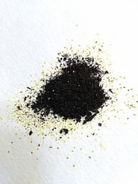
So, Lets Get Started with Fetching a Glass Jar (Preferably Heat resistant) and come powder of Ferric Chloride. Mix them in 1:5 parts of FeCl3:H2O.

NOTE This is a EXOTHERMIC Reaction so do it deliberately. Add the crystals first then mix water slowly.

NOTE FeCl3 is extremely irritating so use Gloves.

-->+Water ==imageimageimage


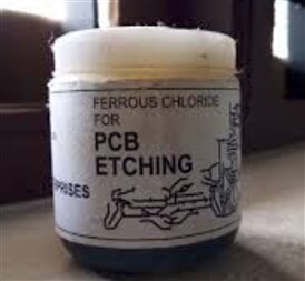
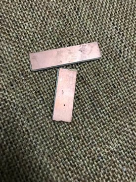
Second Step is cut the Copper Board using paper cutter; Make grooves in front as well as Back and simply snap them. to get the pieces as shown in the image. After snapping, take a dish scrubber and gently scrub the copper surface till it is shiny.

image

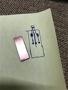
Third step is to feet the components you want to use on a piece of paper and mark the leads on paper, then draw the connections on the paper.

NOTE DONT CRISS CROSS The connections, they will come up as shorts In final design.

P.S. You can also be more artistic by making designs and writing texts. as you can see below in image image

imageimage

Fourth step is Etching. Take the Solution created and place the board upside sown. I.e. the shiny side inside the solution and let the board float on the liquid, Do regularly check the echoing process by removing board and inspecting. Keep etching till you can no longer see the copper.

NOTE while etching, the places you had drawn using marker will be intact and rest of the copper will slowly turn into a mate copperish look.

image

Fifth STEP is cleaning. I used a AfterShave for this as it has high concentration of Alcohol (One of the universal solvent) and it smells Awesome image

image

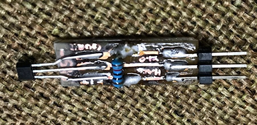
Pre Final STER is to check the board for stupidity image \

As you can see in the Images below I had Written SbSr right where my Hall effect sensor would come an di was stupid enough to remove the marker from it exposing the copper. So I had to use some Insuating tape to hide the text image Stupid me.

imageimage

Final step is to Solder the board and test image Get your cheep ass soldering station and get on to it.

image

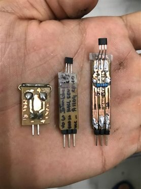
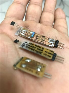
I made another one just out for redundancy. Below are some other boards I made while testing image

imageimageimageimage


So with the PCB's sucessfully fabricated, it time to test them image Tune on for next post on that image


Regards,

GS Gill

  • Sign in to reply

Top Comments

  • DAB
    DAB over 7 years ago +1
    Nice board work. DAB
  • DAB
    DAB over 7 years ago

    Nice board work.


    DAB

    • Cancel
    • Vote Up +1 Vote Down
    • Sign in to reply
    • More
    • Cancel
element14 Community

element14 is the first online community specifically for engineers. Connect with your peers and get expert answers to your questions.

  • Members
  • Learn
  • Technologies
  • Challenges & Projects
  • Products
  • Store
  • About Us
  • Feedback & Support
  • FAQs
  • Terms of Use
  • Privacy Policy
  • Legal and Copyright Notices
  • Sitemap
  • Cookies

An Avnet Company © 2025 Premier Farnell Limited. All Rights Reserved.

Premier Farnell Ltd, registered in England and Wales (no 00876412), registered office: Farnell House, Forge Lane, Leeds LS12 2NE.

ICP 备案号 10220084.

Follow element14

  • X
  • Facebook
  • linkedin
  • YouTube