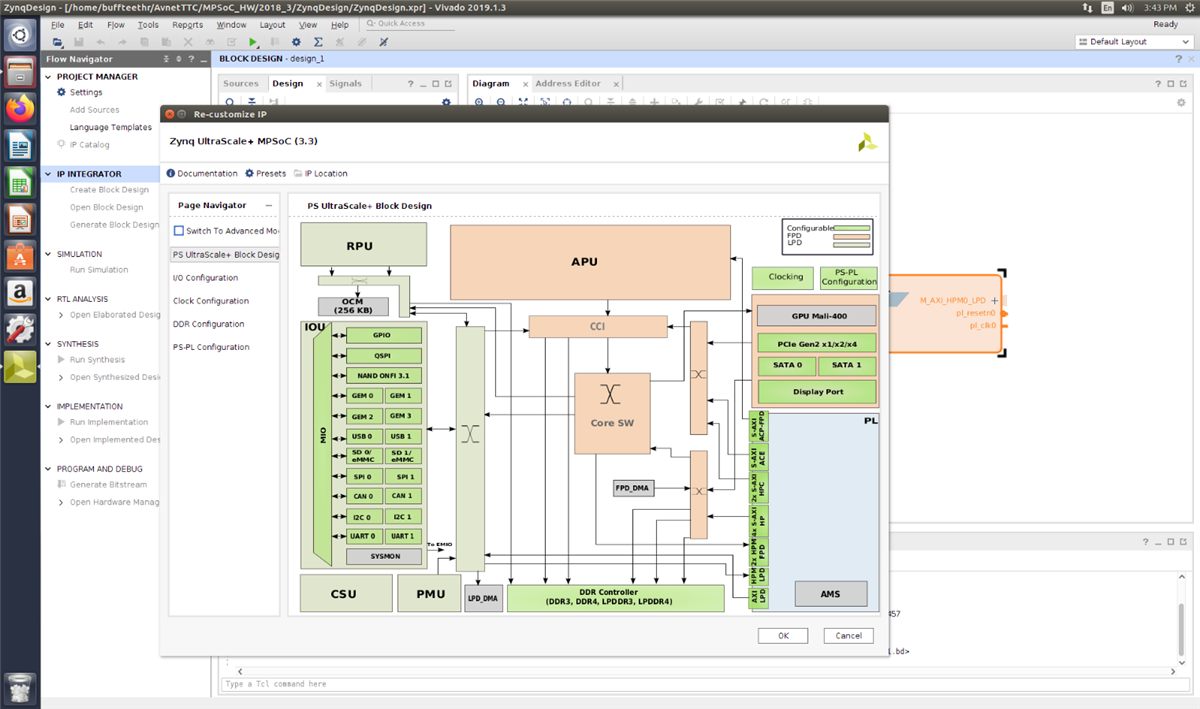
Lab 1: Vivado includes all the required tools for creating new FPGA and SoC designs as well as the Software Development Kit (SDK) for developing software. The Zynq MPSoC Processing System (PS) has a configurable set of built-in peripherals as well as direct access to Programmable Logic (PL) that can build any custom IP. The PS may be used without anything programmed in the PL. However, in order to use any soft IP in the PL, or to route PS dedicated peripherals to device pins in the PL, programming of the PL is required. The lab illustrated an example of how to create new Zynq projects using UltraFast Design Methodology within Vivado.
At the end of the lab I learnt how to:
• Create a new project in Vivado
• Target the Zynq ZU3EG device
• Create a new block design utilizing Vivado’s IP Integrator design flow
• Add an Embedded ARM processor core to the project
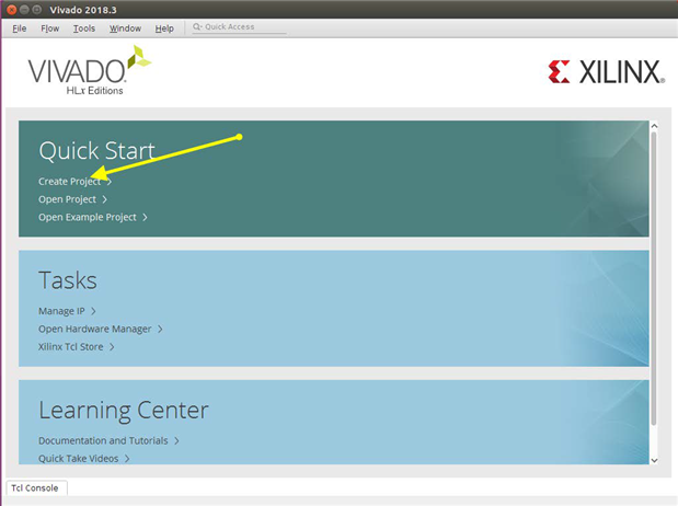
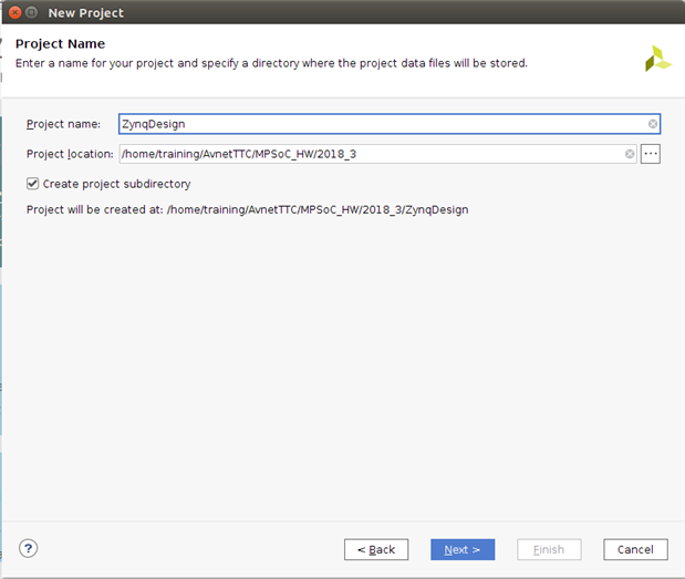
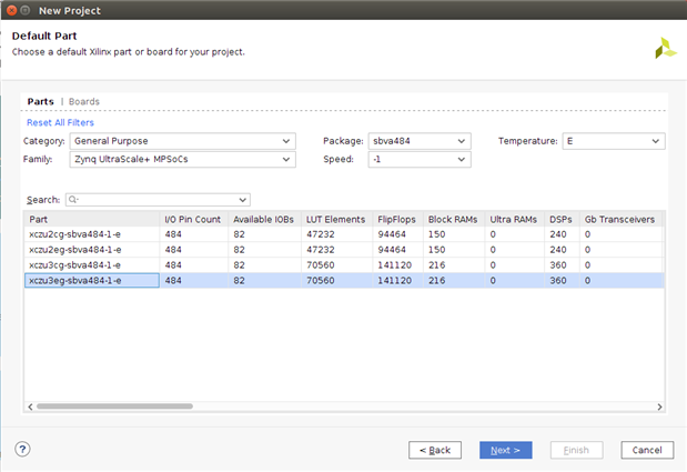
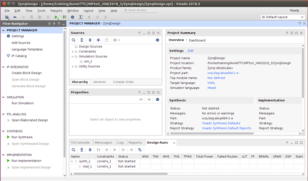
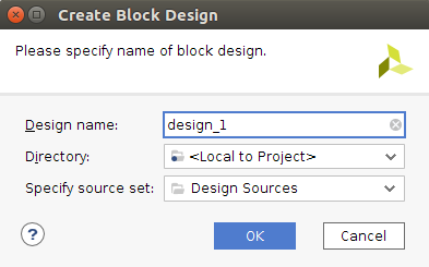
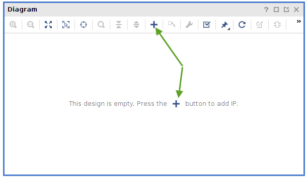
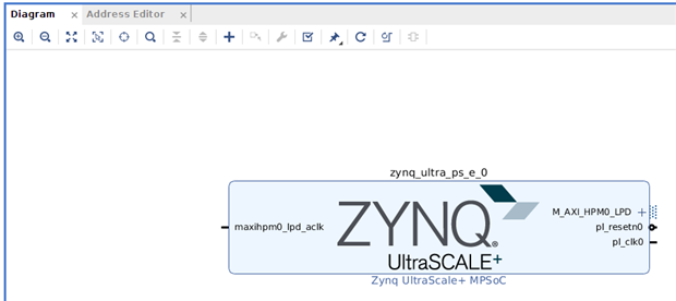
It was a fairly straight forward process that walked you through setting up your hardware project. See the images above.
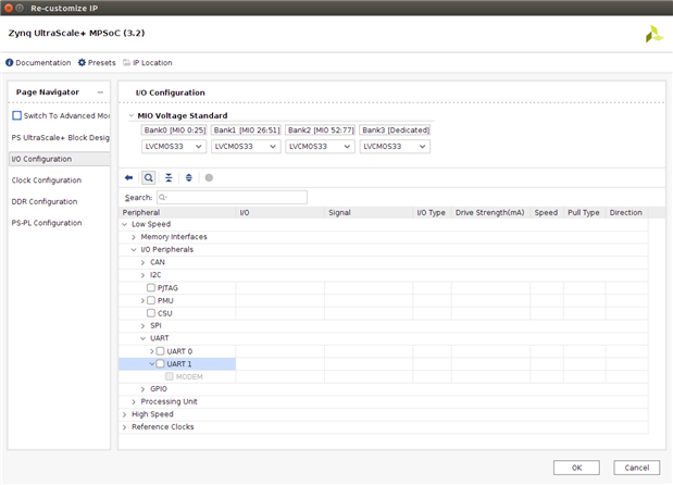
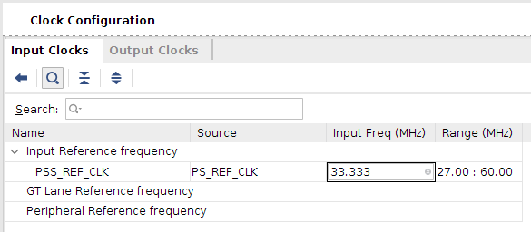
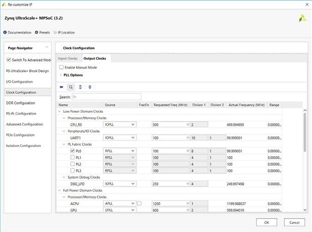
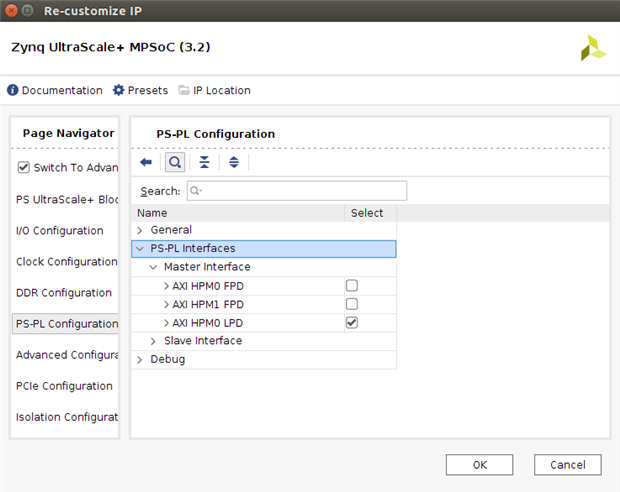
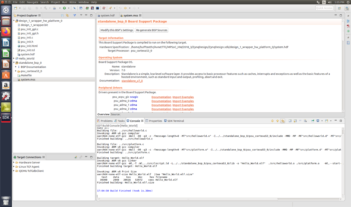
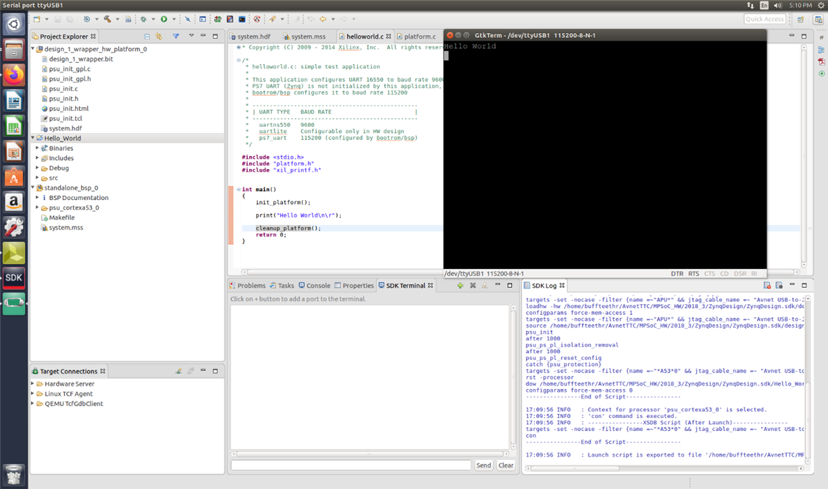
Lab 2 takes over where Lab 1 left off, in which an ARM Processing System was added to the IP Integrator block design. In this lab, I configured the processing subsystem by adding a UART peripheral, configuring internal clocking resources, and setting up our DDR memory controller. The design was then exported to the Software Development Kit (SDK) and a simple Hello World application was created.
At the end of the lab I learnt how to:
• Enable and map a Zynq MPSoC PS UART peripheral
• Configure Memory and Clocks for the Zynq MPSoC PS
• Build the hardware platform
• Export a design to SDK
• Create and run a Hello World application