


These first few labs have been about getting up and running on the Xilinx SDK and getting familiar with the SDK environment.
SDK First Impressions
The SDK is built on the Eclipse IDE platform. I have had very little interaction with Eclipse in the past, but I'm liking it quite a bit already. To an inexperienced user, it's hard to tell what features are native Eclipse and what features have been added in by Xilinx. Overall, the feel and design flow seems user-friendly and intuitive. My favorite feature is the context popups you get when hovering over different elements in source files. You can see macro expansion (i.e. what values / definitions macros are initialized with), function definitions / prototypes, and I even saw info on a string (within a print statement), but haven't been able to replicate it for a screenshot. Below are a couple examples (Fig 1 and 2). Once the popup appears, you can move your mouse over it in order to expand the popup or scroll to see more context. Definitely a handy feature!
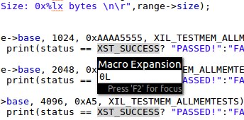
Fig 1. XST_SUCCESS Macro Expansion
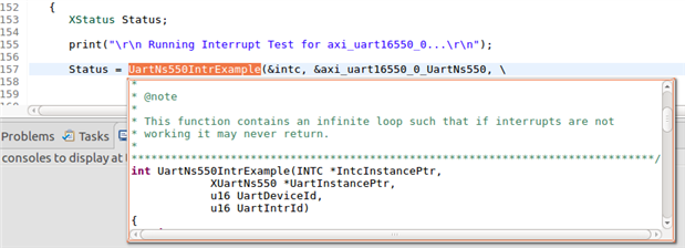
Fig 2. Hover over function shows function definition
Labs 1 and 2: Hardware Platform
In Labs 1 and 2, we learned about the MPSoC hardware platform and hardware definition file (HDF). The hardware platform contains configuration parameters for the ARM processing system (PS) and the hardware design to be loaded in the programmable logic (PL). The HDF is an archive exported from Vivado containing the hardware platform configuration.
The HDF is an archive containing various files pertaining to hardware configuration. These files are specific to the Ultra96-V2 board and would vary depending on the hardware platform being targeted The HDF contains the following:
1. Hardware hand off (hwh): Used by SDK to create a board support package (BSP).
2. _bd.tcl: TCL file for re-creating the MPSoC block design
3. _wrapper.bit: programmable logic (PL) configuration bitstream which is used to configure the PL / FPGA fabric at power-up or via JTAG.
4. _init.c: Register setting definitions for initializing the ARM processing system (used to create bootloader)
5. _init.h: _init.c header file (also used for bootloader)
6. _init.html: Contains info on ARM processing system (PS) configuration for a given platform (register settings, etc)
7. _init.tcl: TCL equivalent of _init.c; used to init ARM when using JTAG/debugging via SDK
8. _init_gpl.c: Same as _init.c but includes GNU GPL header
9. _init_gpl.h: Same as _init.h but includes GNU GPL header
10. sysdef.xml: system definitions, parameter definitions for all files in hardware archive
Lab 2 walked through creating a workspace and importing the HDF into SDK. A workspace typically contains one imported hardware platform, one or more BSPs, and various application projects targeting the board. We explored the contents of the HDF, including the address map for the board and the IP blocks included in the design. Detailed information about the IP blocks is located in the Zynq UltraScale+ technical reference manual, Xilinx programmable logic documentation, or for custom IP, from the designer of said IP.
Lab 3: Board Support Package
Lab 3 went over the details of a board support package. A BSP is a collection of low-level libraries and drivers enabling software applications to interact with different features of the MPSoC and peripherals of the board. Applications run on top of this BSP layer. The lab introduced a standalone BSP which can be built with many Xilinx software libraries. These libraries enable features like standard I/O, networking, file system, external FLASH interface, configuration of the PL directly from the PS, in-system FLASH interface, power management and encryption.
The BSP documentation in Xilinx SDK is very good. The BSP description file (system.mss) lists each peripheral with links to its respective documentation. The documentation lists available APIs, data structures, a list of files associated with the driver, and examples.
Lab 4: Developing an Application
Lab 4 showed the process for creating an application in Xilinx SDK. For each example application that was added, the standalone BSP generated in Lab 3 was used. We added the obligatory "Hello Zynq" (Hello World) example application, as well as a peripheral test application and some memory test applications.
We examined the default linker script created when adding an application. This script contains a list of available memory regions, stack/heap size settings, and memory region mappings for each application section. We also played with creating a new linker script. Here we can control where each section (code, data, stack/heap) is placed in memory (on-chip, DDR, or block ram), as well as stack/heap size.
With each change to source or linker script, etc., the SDK recompiles the application project. This seems like a convenient way to quickly catch bugs caused by typos.
***One question I had in this lab was how we would've known on our own that the first 0x50 bytes of DDR were reserved for exception handling vectors. I'm not sure if this is specific to the DDR or a function of the board design, but it was an interesting detail to learn.
Lab 5: Connecting SDK to Hardware
Alright, now we're working with hardware! This lab walked through the debug environment in Xilinx SDK.
The debug environment seems very powerful. The JTAG debug interface allows for viewing register / memory contents, configuring the PL with a bitstream, downloading application code to memory, and of course debugging with breakpoints, etc.
Applications can be run standalone (right-click the application and select Run As -> Run Configurations...), or they can be run in debug mode (right-click application and select Debug As -> Debug Configurations...). There are other options for debug, including "Launch on Hardware (System Debugger)", "Launch on Hardware (System Debugger on QEMU)", "Launch on Hardware (GDB)", but these options aren't explored at this point. We walked through creating a new system debugger configuration and then launching the debug session.
When launching the debug session, a new "perspective" is displayed in the SDK which shows many new elements. Source files are shown, with the current line to be executed highlighted in green. A Memory view tab is shown on the bottom right, and other new tabs in the upper right include views of device registers, variable values, breakpoints, etc. as seen in Fig 3.
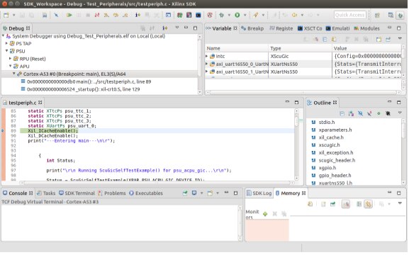
Fig 3. Debug Perspective in Xilinx SDK
I stepped through the Test_Memory application we created in the previous lab. This was the perfect opportunity to add a memory monitor.
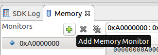
Fig 4. Memory Monitor (Lower right of Debug perspective)
We know from the previous lab that the Test_Memory application first tests the AXI BRAM, followed by the DDR4. The base address for the AXI BRAM can be found in the HDF:
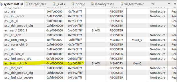
Fig 5. AXI BRAM Base Address in Hardware Definition File
The address listed in the memory map is 0xA0000000 for the AXI BRAM. This can also be found in the variables view in the debug perspective. The "memorytest.c" source file declares a "memory_range_s" variable containing the memory base address:
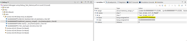
Fig 6. AXI BRAM Base Address defined in program variable (Upper right of Debug perspective)
I set the location of my first memory monitor to location 0xA0000000. I then set break points in front of each memory test function call; the 32 bit test, the 16 bit test, and the 8 bit test:
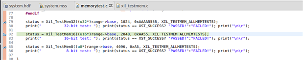
Fig 7. Program break points
Using "Step Over" will not enter function calls / loops, but I wanted to step through some of the memory test application. For this, I used "Step Into":
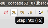
Fig 8. Step Functions in Debug Perspective
This brought me into the "xil_testmem.c" source file, and I could see values being written to the memory addresses in the memory monitor. The following shows a 8-bit write test on the AXI BRAM. Values 0x01, 0x02, 0x03 and 0x04 are written to addresses 0xA0000000 through 0xA0000003, and so-on, as I step through the application:
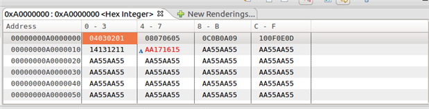
Fig 9. AXI BRAM 8-bit word memory test (stepped)
I added another Memory Monitor for the DDR4. From a previous lab, we know DDR4 starts at address 0x0. This can be seen in the HDF file shows in the debug perspective:
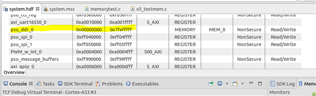
Fig 10. DDR4 Memory Address
In the previous lab, we also learned that DDR4 address locations are reserved until 0x50, which can be seen back in the variable view. I added the Memory Monitor for address 0x50. The following are screen shots captured while stepping through the 16-bit and 32-bit memory test on the DDR4:

Fig 11. DDR4 16-bit word memory test (stepped)
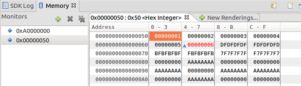
Fig 12. DDR4 32-bit word memory test (stepped)
And that's it! It was nice to finally get some more hands-on with the hardware in this lab.
The level of instruction has been very detailed so far. The videos give a brief overview and then the lab documentation really dives into the details. I'm excited to keep progressing through the rest of these SW labs and I can't wait to get to the HW labs!
-Phil
Top Comments