


Introduction
In this blog I will go over the Hardware module of the Ultra96-V2 training. I will change my approach slightly compared to my Software posts: instead of going through each lab, I will cover the main concepts I learnt form the lab exercises and lectures.
So, here are the 2 things I want to talk about this time:
- IP Integrator;
- AXI interface debugging.
IP Integrator
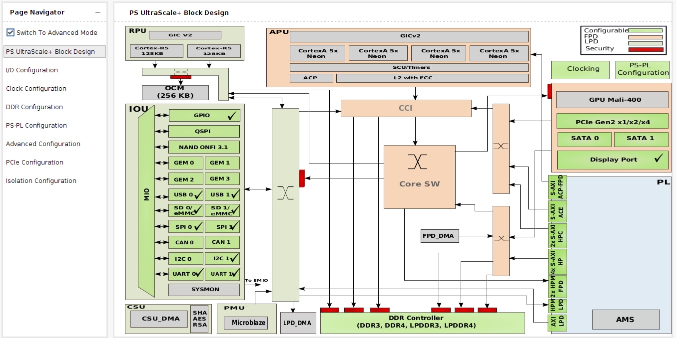
Since it is more and more common for PL and PS to be combined within one module, knowing how to work with IP Integrator became an absolute must. It is incredible to what extent the complexity of such a system as Ultra96 that includes PL, 2 processors and a GPU is abstracted away by this tool.
In this case, the core IP block in the design is Zynq Ultrascale+ MPSoC. I found the graphical representation of the internal blocks very intuitive to work with and it gives a good overview of the current configuration. Most of the options like clock frequencies and active interfaces are configured from the menu on the left.
I liked the way the lab instructions were written for the advanced settings of the Zynq module. Not every selected clock frequency or pin allocation was explained in detail; however, references to the corresponding sections of the datasheets were given. In this way, the instructions are not overloaded with content but still give an opportunity to get a more detailed understanding of what is happening.
If there are no custom IP blocks in your design, I would say that you will spend most of the time on Zynq configurations. Adding blocks already included in the Vivado IP library is relatively straightforward, and “Run Block Automation” feature helps a lot. Therefore, for a very basic project, the design workflow will be approximately as follows:
- Add Zynq MPSoC to the block design;
- Configure the DDR memory;
- Setup System Clocks;
- Select interfaces and map them to IO;
- Add peripherals;
- Connect the blocks (with the Block Automation);
- Validate block design (another Vivado built-in feature);
- Generate HW wrapper;
- Generate bitstream;
- Export HW and launch SDK.
I have never tried to package any of my designs as IP blocks with AXI interface before. Therefore, I was very glad to discover that the largest lab in the course is dedicated to this process.
We start off by creating a new IP with an AXI interface. In the lab exercise, we are creating a PWM driver for LCD backlight brightness control. Our IP block has the following internal architecture:
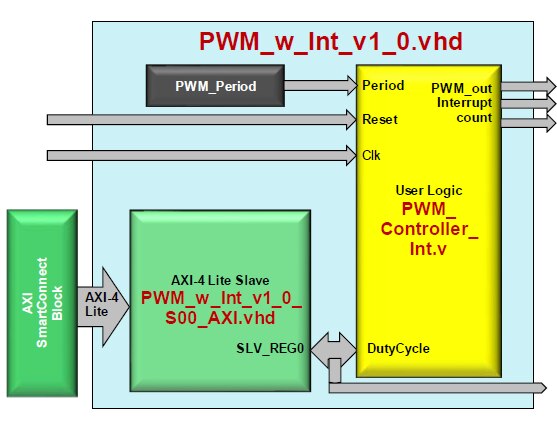
IO:
- PWM_out: The actual PWM output to be connected to the LCD;
- Interrupt_out: An Interrupt that indicates an invalid PWM setting;
- PWM_Counter: The free running PWM counter (for debug);
- DutyCycle: The value passed down from the PS via the AXI interface to control the duty cycle of the PWM(for debug);
Parameters:
- PWM_PERIOD: sets the counter depth of the PWM counter.
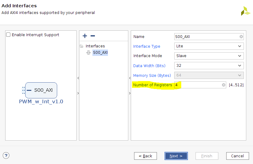
As you can see, the only signal accessible through the AXI interface is the PWM Duty Cycle. Therefore, at least one AXI slave register needs to be added to the IP block. Registers can be added through the GUI as highlighted in the figure below.
I won’t cover the internals of the PWM logic itself. What is more interesting is how to connect that to the AXI interface, so that the duty cycle can be set by the PS. The PWM_w_Int_v1_0_S00_AXI.vhd is autogenerated by Vivado and has AXI interface signals and logic. File also has some placeholders to fill in with user logic. One of the 4 AXI slave registers can be used to receive Duty Cycle setting. A 32-bit wide slave port can be added to the AXI bus port map. It can then be connected to Duty Cycle port of the PWM_controller module in the wrapper.
The IP block can be packaged once all signals are interconnected as desired. In the IP Packaging tool GUI many options can be configured such as what to include with the component (simulation files, synthesis, etc.) and what signals are accessible from outside the block. The resulting IP looks like this:
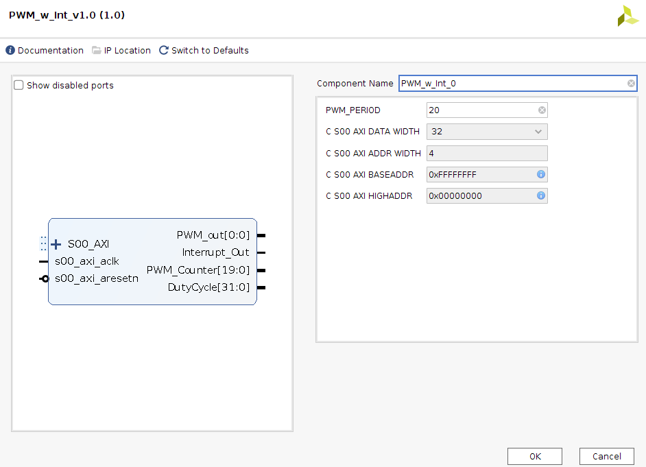
PWM driver is then accessible from the Vivado IP library. It can be added to the Block Design and connected to Zynq MPSoC.
Debugging
Two extra components were added for debugging purposes: Integrated Logic Analyser (ILA) and JTAG AXI. The following is the complete design:
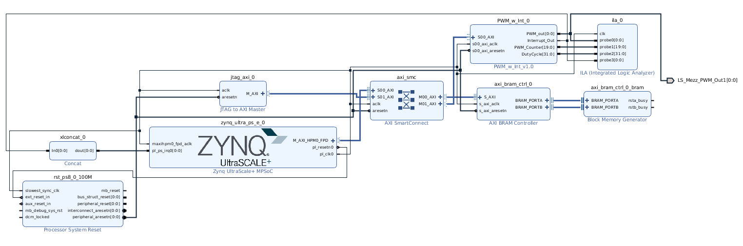
ILA is extremely useful to monitor the internal signals live. In this example, it was used to monitor the Duty Cycle changes based on the user input for the backlight brightness. Since used ILA before, I was more curious about the JTAG to AXI core.
This block allows to manually trigger AXI transactions and inspect their behaviour. This can be very handy to verify communications between various AXI peripherals. In this example, contents of AXI connected BRAM was modified by performing AXI write operation.
Create AXI write transaction: create_hw_axi_txn write_bram [get_hw_axis hw_axi_1] -type WRITE -address 00a0000000 -len 4 -data {44444444_33333333_22222222_11111111}
- hw_axi_1: AXI-JTAG module instance name;
- address: address in the BRAM;
- len: number of 32-bit AXI words;
- data: data to be written to BRAM.
Then run_hw_axi [get_hw_axi_txns write_bram] command can be used to trigger the write transaction we previously created.
The read operation is very similar. Create Read transaction:
create_hw_axi_txn read_txn [get_hw_axis hw_axi_1] -type READ -address 00a0000000 -len 4
Trigger Read operation:
run_hw_axi [get_hw_axi_txns read_txn]
Summary
I never realised how powerful TCL is within Vivado and how many things can be done with such commands.
Overall, I found the Hardware course very informative, even though the first few labs were very similar to the Software module. The labs and lectures helped finally understand how AXI interface can be attached to custom IP blocks. Having also learnt some useful tricks about AXI interface debugging using AXI-JTAG block I feel encouraged to explore TCL scripting more.
PWM with LCD Demo
Top Comments