


This blog is continuing on with the rest of hardware labs.
Lab 5: Adding a PL Peripheral
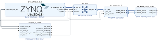
In this lab, we added our first PL peripheral to the hardware design. We added an AXI BRAM controller which allows the processing system to access the programmable logic block ram via an AXI interface, giving the PS yet another source of memory (in addition to the on-chip memory and DDR4 memory on the Ultra96-V2 board). The Xilinx AXI BRAM controller IP allows for configuring AXI protocol, number of BRAM interfaces, data width, and memory depth, as well as error correcting code options.
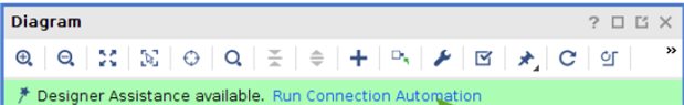
Once the controller IP was added, some additional IP needed to be added. Vivado has a convenient feature called "Designer Assistance" which can automatically add and/or connect certain IP as needed:
 |
In this case, Vivado added a Block Memory Generator which creates instantiations of interfaces to the BRAMs.
The final pieces needed to access the BRAM were an AXI master, a fabric clock and a fabric reset configured in the PS. We added the AXI master and fabric reset in the MPSoC+ configuration block under PS-PL Configuration, and the clock in the Clock Configuration.
Again the Designer Assistance option was available. Running it added an AXI SmartConnect block (connects AXI master in PS and AXI slave BRAM controller in PL) and a Processor System Reset block. After this was all done, we generated the bitstream.
 |
NOTE:There was one lab instruction that seemed out of order in this lab. Step 15 in experiment 2 viewed the BRAM settings which should have been 128 write/read width and 1024 write depth. Mine initially showed 32 write/read width and 8192 write depth. This step said these parameters are inherited from the BRAM controller IP and updated when the design was validated. It wasn't until after step 17, where we were instructed to validate the design, that the parameters did indeed update and match what was shown in step 15.
Lab 6: Improve PS-PL Dataflow using DMA
This lab explored using DMA to improve dataflow between the PS and PL.
We started a new application in SDK and imported the dma_test.c source example. This exercised data transfers of varying depths through different datapaths on the Zynq MPSoC+. One datapath was through the processor (cache coherent interconnect) and the other was through DMA.
The application showed multiple orders of magnitude improvement on data transfers via DMA vs data transfers through the processor, which really illustrates the power and efficiency of DMA.
Lab 7: Adding Custom IP to Vivado IP Catalog
This lab was interesting because it showed how to package custom IP so it could be selected through Vivado's IP catalog to be added to the hardware design. We packaged the PWM with interrupt IP, which was used throughout the SW labs. There are different packaging options. In this case, we selected create AXI4 peripheral, since we would be using the AXI interface to communicate from the PS to the PL.
Once added, we had to add a definition for this IP. It is custom logic, after all, so we have to provide the definition. This consisted of a top-level which instantiated an AXI interface, and an area for user logic. The lab instructed to add a component declaration for our user logic component "PWM_Controller_Int". I opted to directly instantiate the logic which is legal VHDL syntax since VHDL-1993. Essentially, with direct instantiation, there is no need for the component declaration. This saves many lines of code, as you don't have to duplicate all the generic/port names for each component you use in your design. One downside to this is the source of the instantiated component must always be compiled before the source where the instantiation takes place. This is fairly standard practice, however, so it's not that much of a drawback. This is shown below with an empty port mapping:
 |
If a component has multiple architectures, one can be specified in the following way:
"entity work.PWM_Controller_Int(arch1)"
This instantiates an instance of "PWM_Controller_Int" using architecture "arch1", for example.
We completed adding any additional required signals and routing all the required signals between our user logic and the higher-level wrapper, and then continued the rest of the IP packaging process. We walked through the various facets of IP packaging, including identificatdion, compatibility selection, file groups, parameter customization, ports/interfaces, and addressing/memory. When finished, we added the custom IP to the block design and made the required connections.
Finally, we added a few IP blocks which could be used to debug our design. One was an integrated logic analyzer (ILA) and the other was a JTAG-AXI core. The ILA allows us to live probe signals internal to the programmable logic and display them in a waveform display. This block had a configurable sample depth which acts as a resolution adjustment. The JTAG-AXI core allows us to control AXI transactions via JTAG using TCL commands in Vivado. This was all installed in preparation for the next lab.
I had a couple issues with this lab that I'll chalk up to user error.
I had a conflict when adding the packaged IP to the top level design. In the hierarchy, I had PWM_w_int showing up in multiple locations (under the top-level design and in a separate place). I ended up deleting everything related to PWM_w_init in the top-level until the only thing left was a missing source corresponding to PWM_w_int showing in the hierarchy. I added the packaged IP directly to this missing source placeholder and everything seemed to behave after that. I think I followed the directions precisely, so I'm not sure what the issue was.
Additionally, there were some manual connections made between IP blocks in the block design. I was trying to be very precise, but it seemed very easy to make an incorrect connection between ports. I'm certain the connection snapped to the wrong location a few times even though I released it over the right connection. This caused the warning as shown below:
 |
Lab 8: Zynq Hardware Design Debugging
In this lab, we utilized the debugging IP added in the previous lab: the integrated logic analyzer and the JTAG-AXI core. We created a new SDK application and imported an LCD_Backlight_Control_int.c source in order to change the PWM of the backlight on our mikroBus LCD display.
The hardware manager in Vivado provides the interface to the ILA IP in the design. There are various trigger options for starting the ILA sampling. One is called "Trigger Immediate", which is basically a manual trigger (i.e. starts when the user clicks the button). Various automatic triggers can also be set. In this case, we set a rising edge trigger on the PWM interrupt_out signal and set the trigger to occur in the middle of the sample window (i.e. 1/2 the sample window is prior to the trigger, and 1/2 is after). With this trigger setting, we could see an interrupt triggered by the PWM IP when an invalid value was entered in the software application. When a valid value was entered, of course, no interrupt was triggered.
Next, we interacted with the AXI-JTAG core via the TCL console in Vivado. This IP core allowed us to initiate AXI transactions with the PWM interrupt IP and the AXI BRAM IP. We created a transaction to write PWM values to the PWM IP and to write new data values to the AXI BRAM IP.
I had a small issue using the AXI-JTAG core, as I found I had incorrectly set the address space for the PWM IP. I was able to update this in the JTAG-AXI transaction command in order to write to the actual location I had set for the PWM IP. Luckily I had not overlapped memory space belonging to another peripheral.
Lab 9: The Power of TCL Scripting
This was the final hardware lab. Experiment 1, step 5 instructed us to edit the TCL script to increase the number of jobs used to generate the bitstream output. This step did not mention the name of the target TCL script to modify. The next step (6) said to source the TCL script "lab9.tcl", so I figured this must be the script referenced in step 5. Indeed, this was the intended script. I also had to rename several paths in the script, as they contained the "training" example path which I had renamed to something else in my own projects.
Most of this lab consisted of walking through the TCL script and in order to understand the different functions being performed by the script. There are Xilinx TCL functions for basically everything you could want. One interesting point was that the script removed the debug IP (ILA / AXI-JTAG) from the design automatically. In addition, the script enabled RTS/CTS signals on PS_UART_0 which are needed in order to communicate via Bluetooth/WiFi.
TCL can be a powerful tool and can add a lot of extensibility to the vendor tools, but I actually found it a bit clunky for the purpose of generating the build output. If anything was wrong or caused an error, the TCL script did not exit gracefully. Instead, it left elements in the project which were added the previous time the script was run. The next time the script was run, more errors were created when the previous element instances were detected. I suppose this could easily be solved by including a "clean" procedure in the TCL script in case the script errors out, or which can be run at the beginning of the script every time.. Of course, it wasn't until after I went through a series of errors trying to run the TCL script that I read the note saying to use the project included with the lab if any errors were encountered lol!
Summary
The hardware labs gave a good overview of using Vivado. It was nice to get a more well-rounded view of the Zynq MPSoC+ design flow and see how the hardware design flows into the software design. These labs generally went smoothly without too many hiccups and the instruction was mostly clear.