


I think post, I will discuss the latest set of labs in the Path II Programmable series.
In this series, we are provided an Ultra96 board and a series of training modules focused around three areas - Hardware (the FPGA side), Software (the microprocessor side), and Petalinux (the OS side).
Lab 06 - Improving flow between the PS and PL
The outcome of this lab is to describe the differences in how we can architect our system for the best performance; namely the speed of memory transfer using different methods. We start off over in the SDK after exporting the new hardware created in Lab 05 (with BRAM); then we load up a program designed to test the speeds of different types of memory transfer. This will involve the DMA (direct memory access) available in the PS. By using the DMA controller, we can offload memory writes away from the CPU and allow it to do other things until the transaction is complete.
The lab ends with us running a program to test the different speeds compared with each other and we can see the pretty significant results in the serial console.
BRAM to DDR4 transfer
Moving data through processor took 209970 clock cycles
Setting up interrupt system
Moving data through DMA in Interrupt mode took 1250 clock cycles
Transfer complete
Transfered data verified
Improvement using Interrupt DMA = 167x improvement
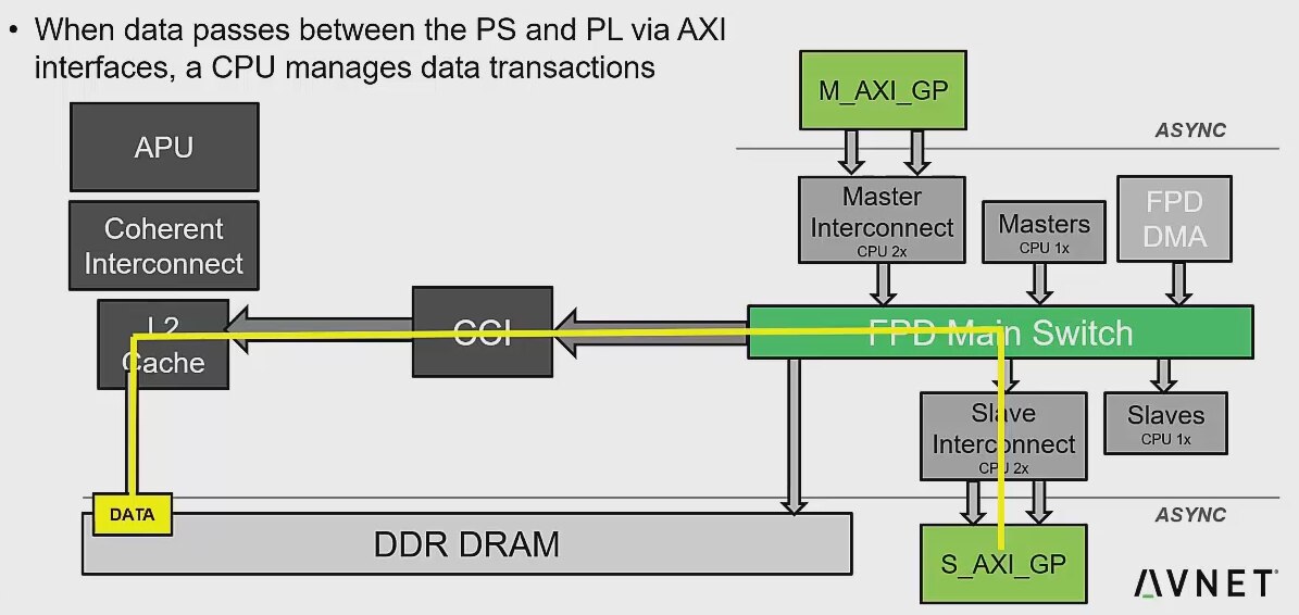
This clip from the lecture shows the 'slow' way to move large amounts of data from the PL in to the DDR. It has to go through the Slave interconnect, FPD Main Switch, then the CCI, L2 Cache, then finally to the DDR. This is a long path, and it requires control from the microprocessor.
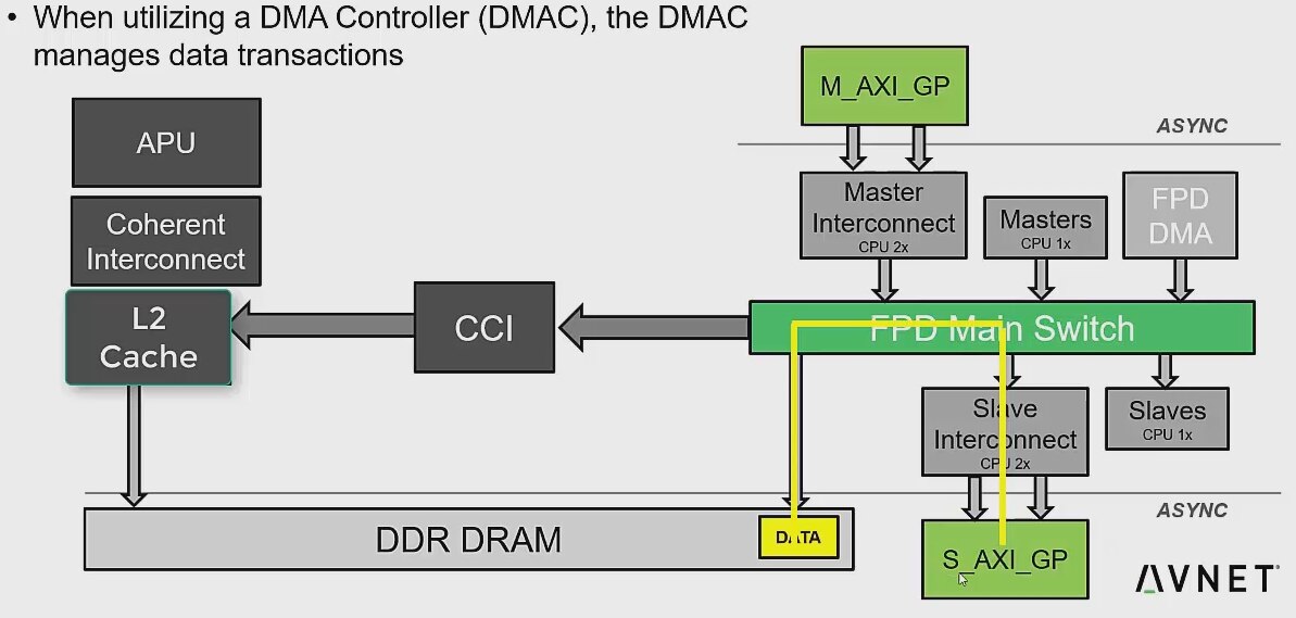
We can shortcut this by using a connection with DMA - Direct Memory Access; and bypass the CCI and L2 go go directly from the main switch into the DDR DRAM. This frees up the processor to do other things while the memory transfer is being done; and provides a significant improvement in performance.
Lab 07 - Creating Custom IP
This lab allows the student to learn about creating custom IP (PL utilities) and adding them to the IP Integrator (IP Library). We have used the library in previous lessons to do things like add our BRAM controller. It can house our IP blocks and make adding them a drag & drop affair once they are created. And of course, this can also be done through the TCL console.
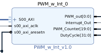
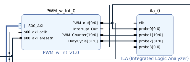
In this lab, we add a PWM controller which will be used in Lab 08 to dim the backlight on an LCD (or not since I don't have the right Click board (yet)). In this lesson, we create the custom IP by importing the C code manually, doing some final configuration, then importing it to the library.
We finish the lesson by exporting the hardware once complete.
Interestingly (for me, anyways) trying to understand which physical pin used was a little convoluted, but simple once I understood it. We link the output port to A6, which comes out the low speed header on pin 29.
But this is how it was explained in the lessons:
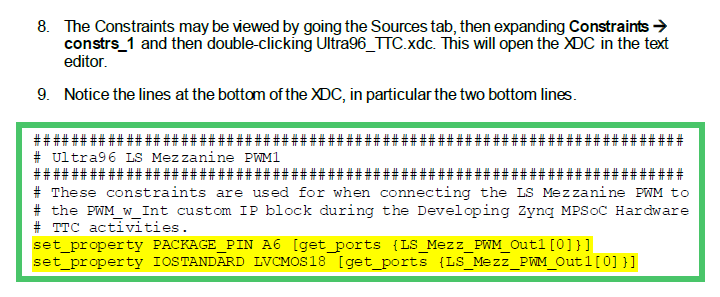
10. The PACKAGE_PIN property sets the LS_Mezz_PWM_out1[0] pin to the physical pin A6 on the ZU+ MPSoC package. As can be seen in either the Ultra96-V1 or Ultra96-V2 schematics, pin A6 is located on Bank 26 and is connected to signal HD_GPIO_6, which is connected to the LS Mezzanine Pin 29, which is connected on the 96Boards Click Mezzanine J1 Pin 29 Signal PWM1, which is the PWM on MikroBUS Site 1, which is where we will plug in the 2x16 LCD later.
So this is a lot more involved than, say, pinMode(A6, OUTPUT) that we would use in Arduino-land; and makes me appreciate how that worked even more.
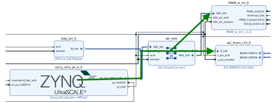
There are two additional things that we add in this lesson - the Integrated Logic Analyzer (ILA) and the JTAG to AXI core.
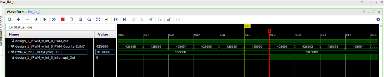
The ILA is a built-in logic analyzer which functions down at the PL level. It makes probing "internal" wires possible and reliable, without needing to surface them on external pins. We find the ILA in the library and add it to our block diagram and wire it to the PWM module.
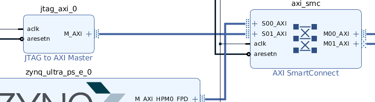
The final component that we add is the JTAG to Axi connection. This will allow manual probing and forcing inputs/outputs via the TCL command line.
We will learn more about these in the following lesson; but for now we export the hardware and switch over to the SDK; but we finish the lab by running the PWM controller from GKTerm and the SDK.

Lab 08 - Vivado Hardware Manager
Lab 08 focuses more around the implementation and debugging of designs. By learning about the integrated Logic Analyzer from within Vivado and the JTAG to AXI interface, we are able to see into a program as it is running, probe internal signals, and manually see and update values that our logic is currently using.
The ILA works much like physical logic analyzers, but has a few distinct advantages - the most major of which is that it is internal on the FPGA. This means that we can probe things like interrupt lines and memory locations that we don't have physical access to. In the PWM example, we are able to see the physical PWM output signal as well as an internal interrupt and a counter register. This just wouldn't be possible with any other external means.
JTAG to AXI
The idea of the JTAG to AXI Master connection is to give a manual method of interfacing with the AXI bus. This means we can query/update memory registers as required to force certain conditions or read the status of registers.
These images illustrate the differences -
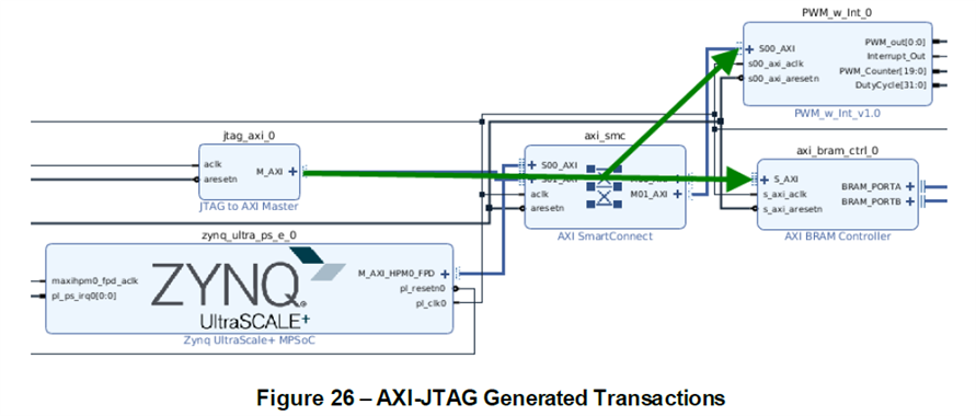
The figure on top shows how in our example, the PS will be typically generate the AXI commands into the AXI bus; but by adding a new master on the bus (JTAG to AXI) then we have a second method; and this is brought out to the engineer back in Vivado through the TCL console.
reset_hw_axi [get_hw_axis hw_axi_1]
create_hw_axi_txn write_txn [get_hw_axis hw_axi_1] -type WRITE -address 00a0004000 -len 1 -data 000A1220
run_hw_axi [get_hw_axi_txns write_txn]
set_property DATA 000FFFFF [get_hw_axi_txns write_txn]
run_hw_axi [get_hw_axi_txns write_txn]
Video Overivew
Here is a video overview of these three lessons.