


- HW Lab 7 - Create Custom IP
- HW Lab 8 - Walk Around without Mezzanine Board
- HW Lab 9 - Incorrect Line Numbers Referred in Lab Instruction
- SW Lab 1 to 3 - Preparation
- SW Lab 4 - Explore Further - A Failed Memory Test
- SW Lab 5 -
- Missing Instruction for Setting Up Debug Configuration for Copied Application Project
- Summary
HW Lab 7 - Create Custom IP
HW Lab 7 is much more complicated than the previous labs. We create a custom IP using VHDL and Verilog code. Also complex IPs are used in this lab too. It took 46 min to generate bitstream on my VM (with an Intel Xeon CPU E3-1505M v5 @3.4GHz). 6 out of 8 CPUs and 24GB out of 32GB RAM are assigned to the VM.
Lesson Learned - Case Sensitive Problem
I learned a lesson regarding name case sensitive. There's no consistence in terms of name case sensitive among all parts involved for Xilinx FPGA design. For example, VHDL is case insensitive while Verilog & XDC are case sensitive.
I used name LS_Mezz_PWM_Out1 in constrain file but LS_Mezz_PWM_out1 in block diagram, so the synthesizer gave critical warnings:
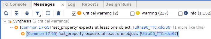
My suggestion: having case sensitive mindset when you name everything (no matter in VHDL, Verilog, XDC, etc.) but NEVER use two names which just have UPPER/lower case difference.
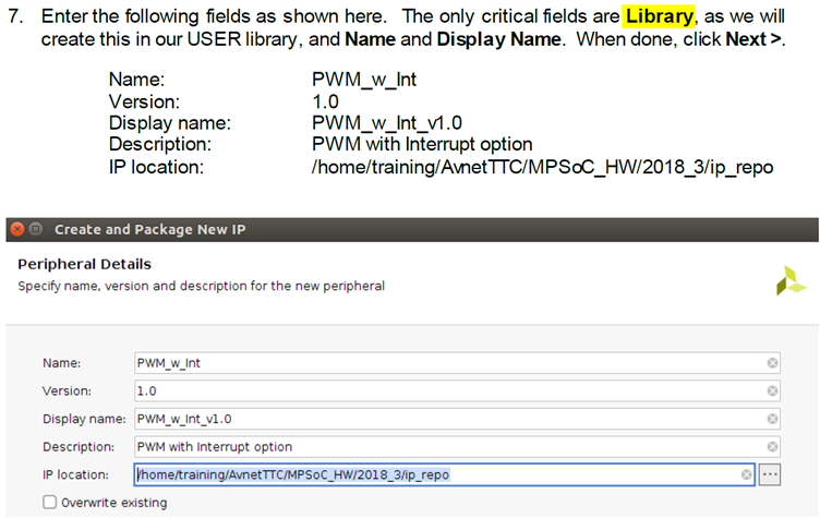
A Missing Field?
HW Lab 7, page 5, there's no field called Library as shown in step 7 below (it may mean the field "IP location"). See the screenshot below.
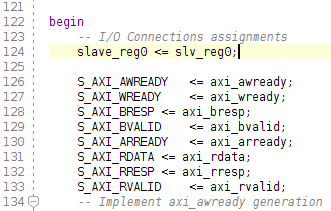
Duplicated Lines
HW Lab 7, page 19, Figure 24 shows duplicated lines and it should look like below
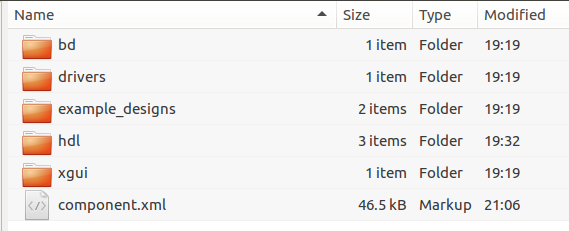
Mystery Folder
HW Lab 7, page 35, Figure 56, somehow I don't have the src folder (I followed the instruction from HW lab 1 to this point without copying anything from provided solution archive) as shown in the lab instruction, but I don't run into any issues without that folder.
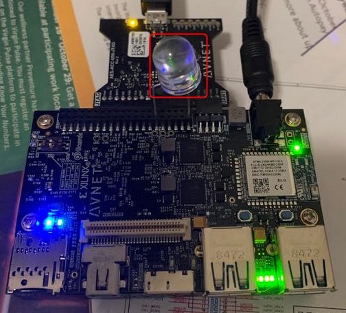
HW Lab 8 - Walk Around without Mezzanine Board
I don't have the Mezzanine (rscasny will send it to all trainees but I cannot wait for this lab) and the LCD mini-Click, so I used a LED (highlighted below).
The following is a video showing the test result when I cycled the brightness from 0 to 9 and back to 0 through the UART console.
Amazing Hardware Debugger & Built-in Logical Analyzer
I heard about built-in logical analyzer before, but this is the first time I actually used. I am really impressed by how easily we can use JTAG and TCL commands to debug the hardware and logical analyzer core to observe the hardware behavior. Great tools for trouble-shooting hardware design.
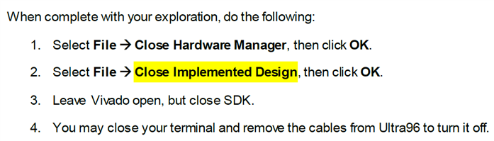
Missing Menu Item?
HW Lab 8, page 22, there's no menu items called "Close Implemented Design". I think it really means "Close Project".
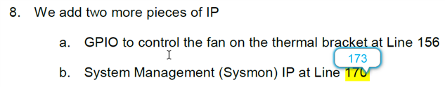
HW Lab 9 - Incorrect Line Numbers Referred in Lab Instruction
There are a couple of labs talking about TCL commands such as HW Lab 4 and this lab. TCL is very powerful script language widely used in EDA software including FPGA design environment. Probably for each GUI operation in Vivado, SDK or SDSoC, there's one or more corresponding TCL commands accomplishing the same task. You can easily exchange your TCL script files for a design with your colleagues while exchanging GUI design files may be troublesome.
I find that from the highlighted line number (shown below) in page 7, HW lab 9 and onwards, all referenced line numbers are offset by 3.
SW Lab 1 to 3 - Preparation
Just like the HW labs, SW lab instructions are very detailed and straightforward to follow. Lab 1 to 3 are the preparation for the labs followed. Since I started from HW labs, I am already familiar with many operations in these three labs.
SW Lab 1 describes the components in the hardware platform archive file. Since I completed the hardware training course, I use the hardware platform file exported from my HW lab 9. If you don't have one from HW lab, you can copy one from the provided solution folder.
SW Lab 2 shows how to create a SDK workspace, import hardware platform designed in HW labs and examine HW platform content and documentation.
SW Lab 3 teaches how to generate a standalone BSP and configure BSP settings such as UART. It also teaches how to examine sample code and peripheral datasheets.
SW Lab 4 - Explore Further - A Failed Memory Test
Mismatch between Instruction and Screenshot
HW Lab 4, Page 3, the instruction doesn't match with the screenshot (instruction says Next but screenshot shows Finish). I followed the screenshot and realized it didn't make sense in the next step (i.e., step 3).

Create an Extra Memory Test Application to Fail
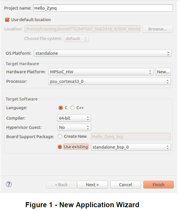
There are three application projects created according to the lab instruction: Hello_Zynq, Test_Memory and Test_Memory_1MB (which is copied from Test_Memory).
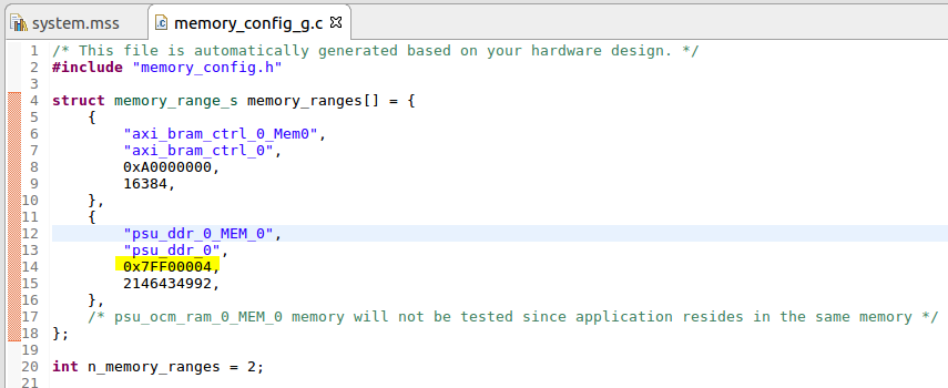
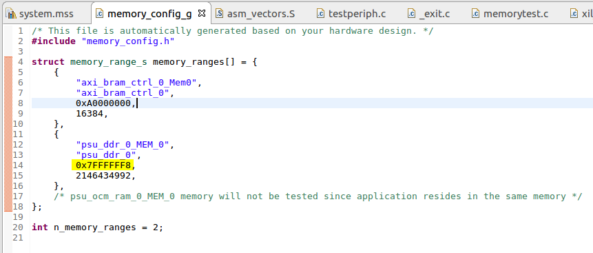
Based on the Exploring Further section shown below, I created an extra application Test_Memory_Failure which is copied from Test_Memory_1MB.
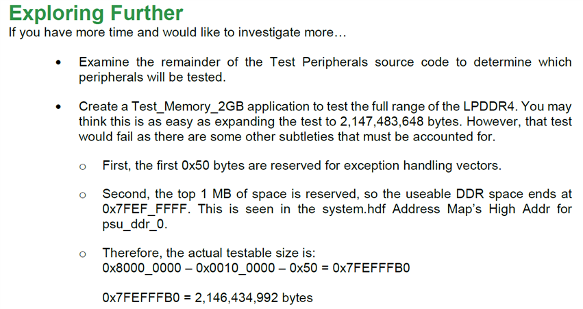
Given the factor that it may take a long time to test 2GB DDR RAM to see the failure, I only test 1MB like the Test_Memory application does, but I moved the start offset much higher (as highlighted below in the following screenshot) and make the test to reach into the reserved top 1MB. Thus I expect the test fail and the failure was verified in the next lab - HW Lab 5.
SW Lab 5 -
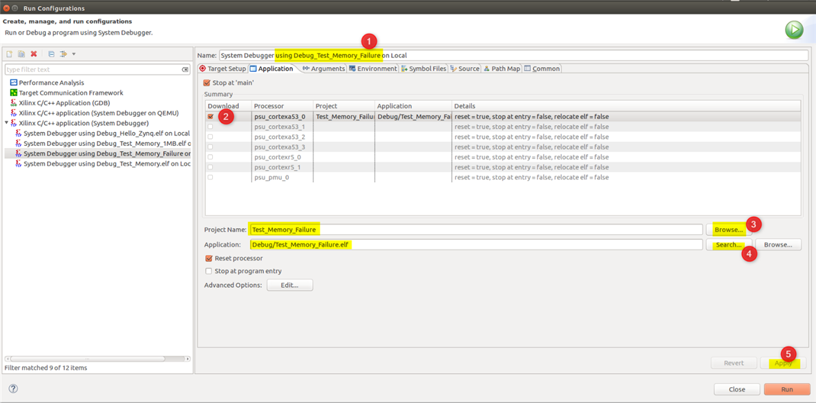
Missing Instruction for Setting Up Debug Configuration for Copied Application Project
When I try to set up the run configurations for both Test_Memory_1MB and Test_Memory_Failure application, the configuration didn't pick up the right configuration name and some settings such as project name and application code. I think the lab instruction forget to mentions this extra step I describe below.
Thus, I have to manually modify those settings as shown in the screenshot below (this is the example for Test_Memory_Failure application)
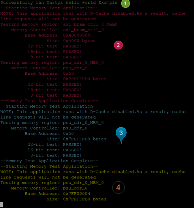
Test Results of Four Applications
Test results in order:
1. Hello_Zynq
2. Test_Memory
3. Test_Memory_1MB
4. Test_Memory_Failure
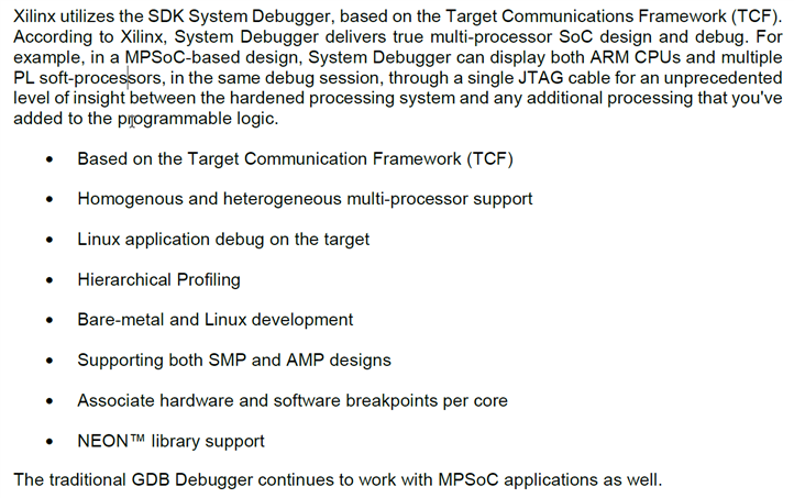
Powerful Xilinx SDK System Debugger
I just realize Xilinx SDK System Debugger is such powerful debugger software based on the following lab instruction. Hope I can exercise its multi-core debugging capability in future projects. A debugger tool supporting Multi-core debugging may cost thousands of dollars.
Debug Example for Test_Memory_Failure Application
I will show the debugging process for the Test_Memory_Failure as a debug example. To speed up the debug process (i.e., shorten the time to generate failure), I increased the start address again (make the first memory access succeed and the second one fail).
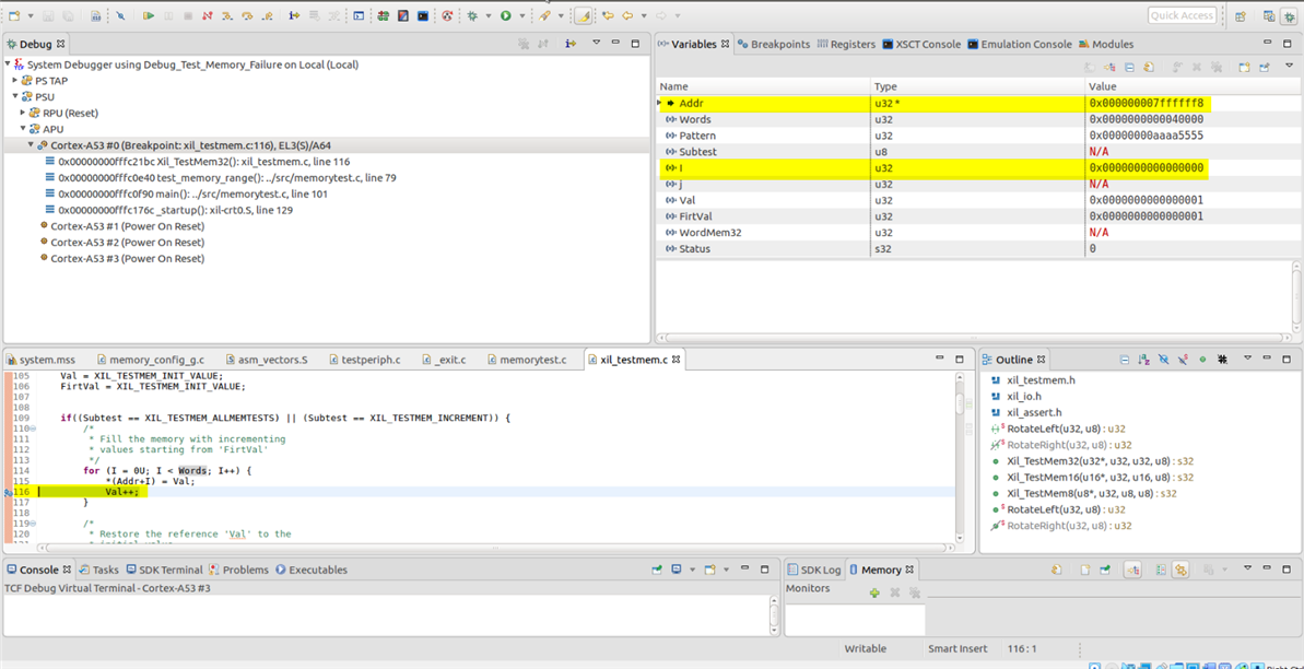
Let's start the debugger, I created a breakpoint at line 116 in xil_testmem.c file where the actual memory access occurs. There are two default breakpoints created by SDK. One is the automatic stop point in main() after the debugger is launched. The other one is in the _exit() function when main() function returns to the standalone OS.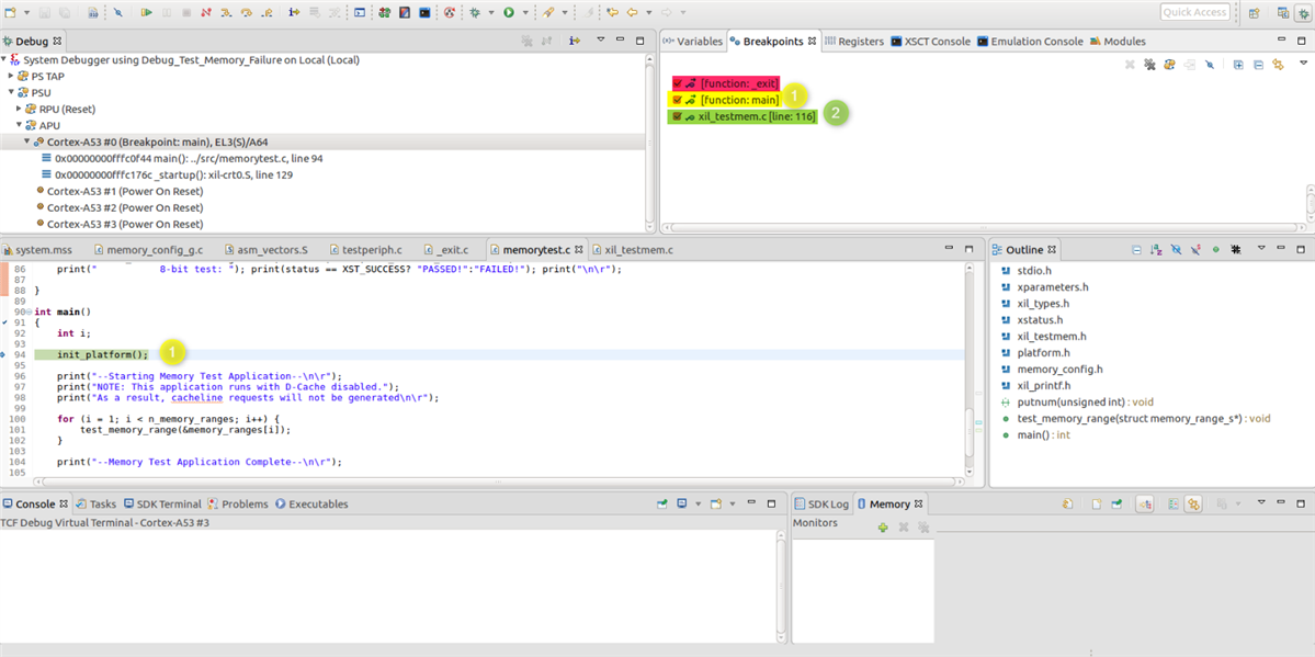
Let's resume the application execution, it successfully stop at the breakpoint I created. Memory location 0x7ffffff8 has been written with content of 0x1.
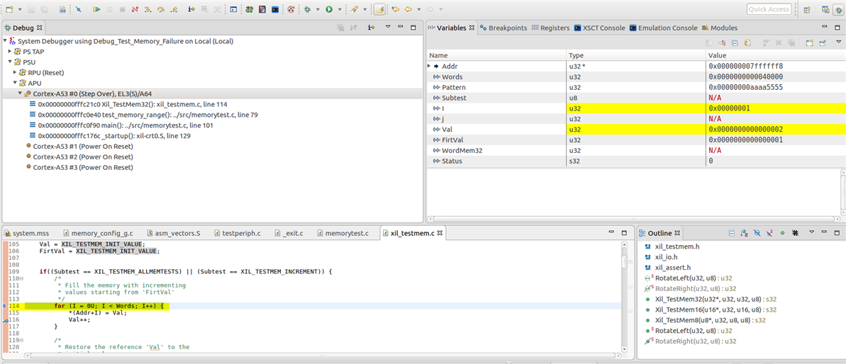
Let's step over once, we see it stops at line 114 (the beginning of the for loop) and variable I and Val are both incremented by 1.
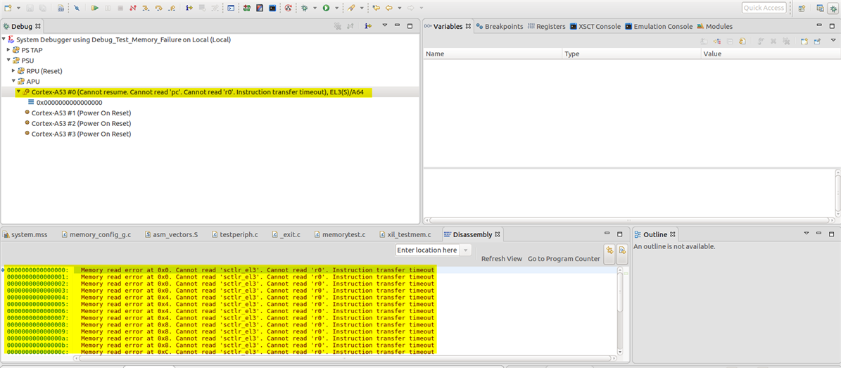
Let's resume the application execution, it shows the memory access error.
Summary
The labs are getting more complicated and lab instructions are well written but not perfect. My journey so far is still pretty smooth. I was able to dig a little bit deeper according to the Exploring Further sections. My blog is based on my personal experience and I cannot guarantee the correctness of the content. Your comments and feedback are always welcome. If any trainee needs help on any lab I have completed, please don't hesitate to ask. Enjoy your training!
Top Comments
-

nerdyupdates
-
Cancel
-
Vote Up
+1
Vote Down
-
-
Sign in to reply
-
More
-
Cancel
-

cmelement14
in reply to nerdyupdates
-
Cancel
-
Vote Up
0
Vote Down
-
-
Sign in to reply
-
More
-
Cancel
-

cmelement14
in reply to cmelement14
-
Cancel
-
Vote Up
+1
Vote Down
-
-
Sign in to reply
-
More
-
Cancel
Comment-

cmelement14
in reply to cmelement14
-
Cancel
-
Vote Up
+1
Vote Down
-
-
Sign in to reply
-
More
-
Cancel
Children