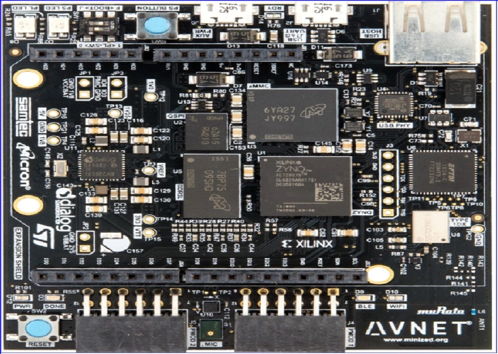
MiniZed is a single-core Zynq 7Z007S development board. With the advent of the latest cost-optimized portfolio from Xilinx, this board targets entry-level Zynq developers with a low-cost prototyping platform.
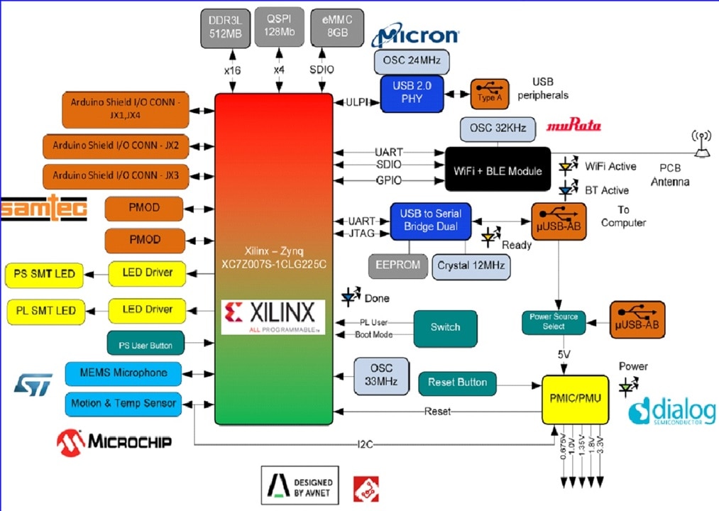
This compact design features on-board connectivity through USB, Wi-Fi andBluetooth. Peripherals can be plugged into dual Pmod-compatible connectors,the Arduino-compatible shield interface or the USB 2.0 host interface. JTAGcircuitry is incorporated onto the MiniZed base board, so with a single micro-USB cable to your laptop you are already up and running. User LED’s, a buttonand a switch allow for a physical board interface.
Micron memory solutions are presented for QSPI flash, DDR3L memory andon-board eMMC instead of an external SD card. The Murata Type 1DX wirelesssolution incorporates 802.11b/g/n Wi-Fi as well as Bluetooth 4.1, whichprovides both Bluetooth Classic and Low Energy (BLE). The integrated powersupply from Dialog generates all on-board voltages, while an auxiliary supplyinput can be used to power designs that require additional current. From STMicro there is an on-board motion and temperature sensor, as well as a digital microphone.
MiniZed provides for an efficient hardware reference design, while it is also an inexpensive board that can be used to run workshops and tutorials. The board aims to showcase the power of Zynq, where the Cortex A9 processor core integrates seamlessly with the programmable fabric to provide signal processing and control solutions. The on-board digital microphone serves as an input for a variety of illustrations of how to implement FIR filters, FFT’s and direct memory access.
MiniZed Block Diagram
SoC IC Package
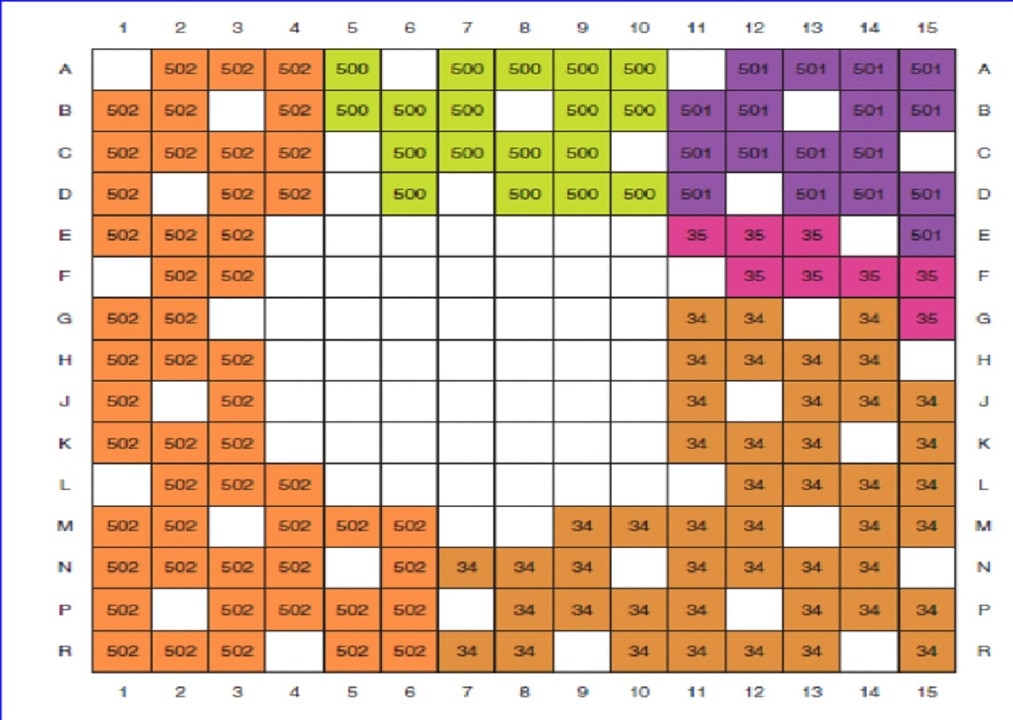
The CLG225 package is a 225-pin 13mm x 13mm BGA with a 0.8mm ball pitch. The image below indicates the locations of the various I/O pins as seen from the top.
Device configuration
Device configuration, i.e. the programming of both the PS and the PL, can be achieved in a number of ways:
̶ Using JTAG via the on-board USB-to-JTAG circuitry to configure the SoC using the Xilinx SDK, which is based on Eclipse (see [8])
̶ Loading an image from the QSPI flash device
̶ Loading the First Stage Boot Loader (FSBL), Second Stage Boot Loader (SSBL) and PL bitstream from QSPI flash so that the Petalinux components can be loaded from either the on-board eMMC or from an external mass storage device such as a Micro SD (uSD) card plugged into a Pmod socket using SDIO
I/O Levels
The MiniZed’s Zynq SoC allows programmable voltage levels for PS I/O pins (1.8V or 3.3V) and for PL I/O pins (1.2V to 3.3V).
Storage
The Zynq PS has 256 KBytes of on-chip RAM. The MiniZed supports 3 types of external memory:
̶ 512 MBytes of DDR3L, which is RAM for data and program storage
̶ 128 Mbits of QSPI NOR Flash
̶ 8 Gbytes of eMMC or SD Card via external PMOD (not included in kit)
Micron DDR3L memory
The MiniZed has a 4Gb (512 MB) DDR3L Micron MT41K256M16TW-107 memory device
̶ The CLG225 package Zynq deice only supports a 16-bit wide memory interface (not x32).
̶ This is a 1.35V device in a 96-ball 8mm x 14mm package
̶ DDR termination voltage and reference are provided by the Dialog DA9062 PMIC ̶ DDR termination voltage of 0.675 V is provided
Micron QSPI flash memory
The QSPI interface is a 3.3V NOR Micron MT25QL128ABA8E12-1SIT flash device.
The MiniZed’s 128Mbit QSPI device can be expected to be large enough to run almost any bare metal application. It is also possible to run Petalinux from the QSPI dependent on how large of a build it is. However in most Petalinux builds the QSPI will be used to store the First Stage Boot Loader.

Optional external power supply
A single USB 2.0 port is only required to provide 500mA. The power budget for the board shows that this power level is easily exceeded when the Zynq device operates under heavy utilization.
̶ A secondary micro USB power input is provided.
̶ When the MiniZed user wants to use more current, he/she will have to provide power from a secondary micro USB input.
̶ In the case of having a large input source, user can populate R114 which will link the two power inputs thus requiring only the single input source.
̶ A “power kit” that consists of a 5V supply and a USB cable can be sold as an add-on item when ordering a MiniZed board.
̶ The two micro USB inputs are connected directly, with each supply being protected by a blocking diode as in the image below.
Module Reset
The DA9062 features a reset controller built into the device. This function is be used for module reset. A reset button is fed into the GPIO2 pin of the power supply, which is programmed with an internal de-bounce function.
The diagram below shows the reset structure


Clocking
The following MiniZed board clock sources are provided
̶ Zynq PS clock - 33.33 MHz Microchip DSC1001DI1-033.3333T Oscillator ̶ An internal PLL can be used to set the operating frequency, up to 667MHz
̶ USB OTG PHY - 24 MHz Microchip DSC1001DI1-024.0000T Oscillator
̶ USB-to-serial FTDI device - 12 MHz Abracon LLC ABM8G-12.000MHZ-B4Y-T Crystal
̶ Murata 1DX wireless module LPO (low power oscillator) - 32768 Hz Abracon LLC ABS07AIG-32.768KHZ-1-T Crystal
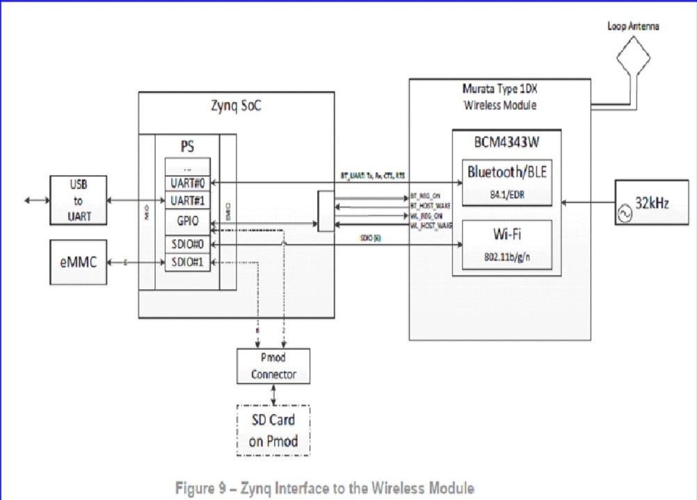
The diagram shows how the Zynq PS peripherals are connected to the 1DX module.
̶ All wireless I/O are connected via EMIO
̶ All 4 UART signals (Tx, Rx, CTS and RTS) are used for the Bluetooth/BLE interface
̶ All 6 SDIO signals are used for the Wi-Fi interface
̶ 4 of the 1DX GPIO signals are connected for handshaking BT_REG_ON BT_HOST_WAKE WL_REG_ON WL_HOST_WAKE
̶ The PCM interface is not connected. This is typically used for driving a Bluetooth speaker directly.
USB Host Interface
This interface is the same as what has been used on previous Avnet boards. It allows USB slave devices such as a mouse, keyboard or USB camera to be connected to the PS. Typically Linux drivers will be used for these devices.
̶ On MiniZed OTG mode is not supported, USB is Host mode only.
̶ The Microchip USB3320C USB 2.0 transceiver uses the ULPI (USB low-pin interface) that the Zynq PS provides.
̶ The USB phy uses a 24MHz clock input.
̶ A USB Type A USB0 connector is provided for these USB slave peripherals.
̶ The I/O voltage, VDDIO, is set to 3.3V. The USB PHY interfaces with PS MIO bank #1 which is shared with the USB-JTAG/UART circuit and is set to 3.3V.
Pmod connectors
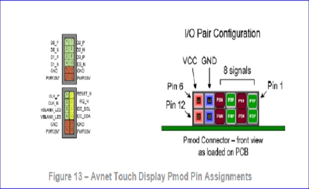
Two 12-pin Pmod connectors are provided. The distance between the centers of the two Pmod connectors is 900 millimeters apart. This is so that modules with two Pmod connectors can also be used. For general details on Pmod-compatible interfaces, refer to [9].
In order for the Avnet Touch Display (see [19]) to be used, the Pmod signals were routed differentially on MiniZed. You must assign the I/Os as TMDS33 differential pairs.
Pull-up resistors
For I2C (as for other open-drain signals) a pull-up is required for the SCL and SDA lines. Those lines can be re-purposed for other uses. Alternatively, weak internal pull-ups in the Zynq I/O cell can be activated.
̶ For MiniZed the assumption will be that most external peripherals that have I2C will have pull-ups on the peripheral itself and that if they are not there, weak SoC pull-ups should be enough.
̶ For the Arduino I2C interface, two 4.75k pull-ups are provided but will not be populated by default. Their REFDES are NTR7 and NTR8.
̶ For Pmod interfaces, no pull-ups will be provided.
Microphone Input
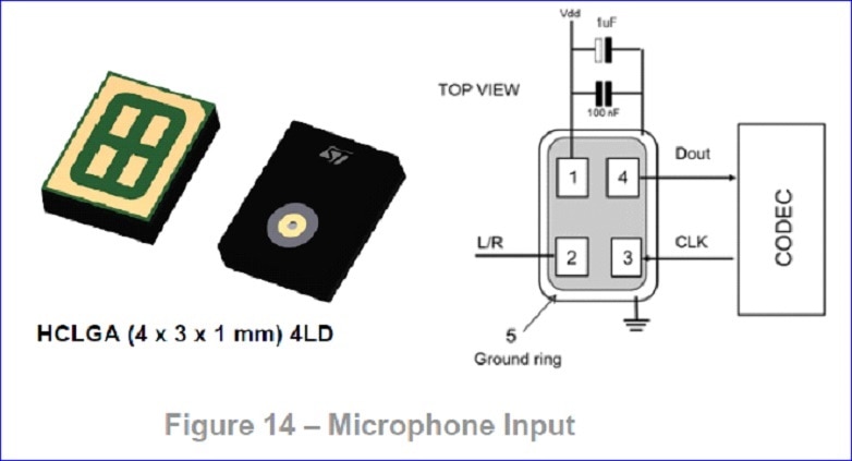
A MEMS (Micro-Electro-Mechanical Systems) microphone is included on the board. This microphone has a simple digital output which allow for audio signals to be processed in the PL.
The MP34DT05 from ST Micro is a 4mm x 3mm omni-directional digital microphone.
The MP34DT05 is a low distortion digital microphone with a 64dB signal-to-noise ratio and –26 dBFS ± 3dB sensitivity
̶ It operates on 1.8V. Level translators are implemented to interface to the 3.3V Zynq interface.
̶ The input clock pin is nominally 2.4 MHz, but it is currently using 2.5MHz to drive it as a divisor of 160MHz
̶ Alternate clock cycles are used to clock data for left and right channels. The output is in PDM (pulse-density modulation). This format can be used to drive CODEC’s directly, but in MinIZed’s case, it is processed inside the FPGA. PDM can be de-modulated by passing it through a Low Pass Filter
Motion & Temperature sensor
The LIS2DS12 from ST Micro is a MEMS 3-axis accelerometer with an embedded temperature sensor.

1.8V supply
̶ 16-bit data
̶ Selectable full scale 2g/4g/8g/16g
̶ 256-level FIFO
̶ The I2C interface is used and will be shared with the Arduino I2C interface
̶ Since this is a 1.8V device, level translators to/from 3.3V logic levels is used
̶ Temperature is relative, not absolute
User interface
LED’s and buttons allow for feedback and control.
Board LED’s
A few single-color LED’s give user indication of the board status:
̶ A green LED indicates board power.
̶ A blue LED indicates that the SoC programming is Done.
̶ Another blue LED indicates that Bluetooth is active.
̶ A yellow/amber LED indicates that Wi-Fi is active.
SoC LED’s
Two bi-filament LED’s are be connected to the Zynq device.
̶ Each led uses two lines and it can therefore be in 4 states: off, red, green or amber.
̶ One LED connects to the PS and the other to the PL. This will allow for GPIO from both sides.
̶ The PL LED is shared with two Arduino pins (A3 and A4). So that these signals do not affect signal integrity, they are isolated by FETs.
Push buttons
̶ A pushbutton switch feeds into the power supply, where it is de-bounced and used to trigger a hard power-on reset.
̶ Another pushbutton switch is connect to the PS and can be used as a MIO input.
Switches
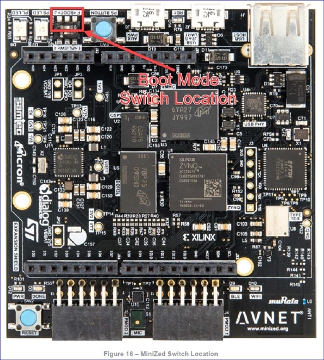
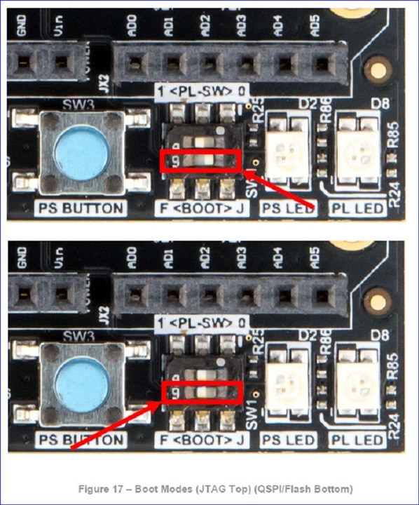
̶ A single surface mount 2 bit DIP switch (dual switch) is installed. ̶ Bit one is used as a user input into the PL.
̶ Bit two is used for JTAG/QSPI boot selection

-

prashanthgn.engineer
-
Cancel
-
Vote Up
0
Vote Down
-
-
Sign in to reply
-
More
-
Cancel
Comment-

prashanthgn.engineer
-
Cancel
-
Vote Up
0
Vote Down
-
-
Sign in to reply
-
More
-
Cancel
Children