


I was able to get a lot of work done over the Thanksgiving weekend. The bulk of the hardware is completed, and now I am shifting the focus over to the software. I am traveling this week so I don’t have much time to divulge much on the analysis of these boards, so I will just post the schematic at the end of the post.
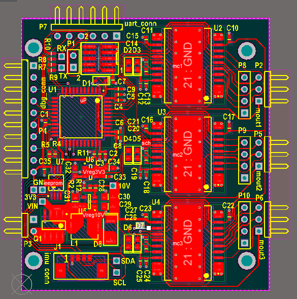
The system diagram that was drawn in the earlier posts has now been realized in schematic form, and you can see that it follows the diagram pretty closely.
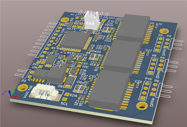
The PSoC is at the heart of the design and will control the motor drivers primarily through PWM blocks. I haven’t tested the PWM blocks, so I’m crossing my fingers that I can figure it out quickly. Other than that, the power supply was covered last week and the remaining portion of the design is mainly test pins and connectors. It took a week for me to find the time to finish doing layout, but it is ready to be fabbed.
There are two main things to look for when doing layout. Once is high current and the other is high speed. In this case, there is no high speed traces, but I am a little concerned about the high current motor drives.
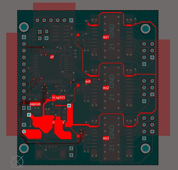
In this diagram, I highlighted the main current path. Since this is 2 layer board design, the return path beneath the main current path should not be interrupted. The hard part was trying to route as much as possible on the top copper so that the bottom copper stays solid under the highlighted nets. Pin swapping is a god-sent feature when doing something like this.
That’s it for now. I’ll be overseas for the week, but I’ll try to submit this to a fab house so that I can get it soon. Hopefully all this effort pays off and the board actually works.
Full schematic below…


