Not inspired by strb's blog.
Expect setbacks and successes because I built my circuit and wrote this blog concurrently.
The first thing that came to mind when I heard about creating something unusual using 555 timer ICs was a direct ADC, and it seemed like a fun project to build!
We are almost there with an ADC because the 555 timer includes comparators and a resister ladder!

The problem with the 555, however, is that there is an SR latch between the output pin and the comparators.
I can emphasise this more clearly if you know how a direct ADC functions.

A resistor ladder, one of the main components of a direct ADC, splits a reference voltage into smaller voltages. I want to divide my voltage into 1V, 2V, 3V, and 4V because the ADC I'm going to build will be 5V.
Following that, a group of comparators will compare the divided voltage to our input voltage. So, if I wanted to make an ADC out of 555, I needed my 555 to act as a comparator, which did not seem straightforward because when trigger(pin no.2) went above 1/3rd Vcc, the latch would set and the output would be logic 1, i.e. Vcc. And until reset is initiated, that state will not change.
Proteus Software is what I'm using to simulate my circuit.
As you can see in the video up top, I'm using a potentiometer to adjust the trigger voltage, and the output is connected to a lamp.
When I increase my voltage above 1.66V(1/3*5V), the latch is set and the lamp turns on. However, when my voltage rises above 1.66V, the SET pin of the 555 latch inside the chip is inactive. Since my output is connected through the latch, I must activate reset to turn off my lamp.
This behavior is different from a comparator. I want the comparator's output to turn off as soon as the voltage reaches a certain level, then only I can make an ADC out of it.
So my first design challenge was to make a Comparator out of 555 IC.
1. Making a comparator out of 555 timer IC:
I came up with a design after brainstorming and playing around with 555. But before I describe my design, I want to describe alternative ways to accomplish this. A comparator circuit that would trigger a reset when the voltage exceeded a threshold would suffice. However, it is 555 Timer Madness ! To accomplish this, I wanted to stick with the 555 IC alone.
So I reasoned that if I repeatedly trigger reset using a PWM wave that can be generated by another 555 timer IC operating in astable mode, the SR latch would reset and my output would no longer be in logic 1 when the voltage exceeds the reference value, which in my ADC design would be 1V, 2V, 3V, or 4V.
Some of you may have already genuinely thought that if I keep resetting my SR latch even when I want my output to be high, my ADC will periodically change its state.


So, how do you deal with a sudden voltage change? A CAPACITOR!
I kept the duty cycle of the PWM above 90% because that would provide a long enough reset active low pulse and would make it easier to compress it on the output using a capacitor. I would require a larger capacitor if it were necessary to compress longer pulses (the more the capacitance larger the size). I adjusted my simulation to use a 10uF capacitor, which was the highest value I could find on hand and experimented with other parameters.
The frequency of the PWM is inversely proportional to the values of R1, R2, and C1 connected to the 555 timer.
Additionally, R1:R2 must be high for a higher duty cycle.
Therefore, I set R1 to 10k and R2 to 220 to achieve a duty cycle of almost 98%.
Now I had to set the C1 value and through simulation, I found out that the higher the frequency of the PWM applied on the reset pin, the easier it was for my 10uF capacitor to flatten it out. So I kept the value of C1 to the lowest value of capacitor I could find with me which was 220pF. Apparently, Proteus hangs when the simulation is run on such a higher frequency so to test it out finally I had to build the circuit.

In the video that is attached above, it can be seen that when I set my potentiometer below a threshold, an LED turns on, and when it exceeds that threshold, an LED turns off. I've thus created a comparator using just two 555 timers and a few passive parts!
2. Making a Flash ADC using 555:
If anybody hates Linear Algebra I'm sorry.
I intended to use four 555 timers for my ADC, which would make my ADC two bits. Given the complexity of my circuit, a reasonable low. Again, it is 555 Timer Madness right!!
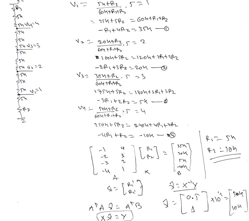
In the 555 timers, on the 1/3*Vcc node, I must divide my 5V into 1V, 2V, 3V, and 4V. As a result, I went back to the material I had just finished studying this semester. LINEAR ALGEBRA!!

Sorry for the bad handwriting. I had to find two unknowns R1 and R2 to make the voltages V1, V2, V3, and V4 as 1V, 2V, 3V, and 4V. So I had two unknowns with 4 equations. I performed orthogonalization to get the best solution.
I was almost done with my ADC at this point. I just had to rig up my circuit. As I didn't have a priority encoder I used an Arduino Uno to do the job.
This is my final circuit.

Failure: This circuit is not going to work.
Utilizing the internal 5k resistors as my resistor ladder for my ADC is not good, because it messes with the Vcc and Gnd of my 555 IC!
Solution: The 555 IC provides a control voltage signal (pin no. 5) and a threshold (pin no. 6) that I can use to control the comparison voltage from outside my 555 IC without messing with my Vcc and Gnd voltages.
The same problem will arise with my previous failed design in that the SR latch will hold onto the value. My high-duty cycle PWM could be fed to the trigger pin rather than the reset pin to solve the problem. By doing this, my output would be complemented, but I can handle that with my Arduino.
So, my final final design is this,
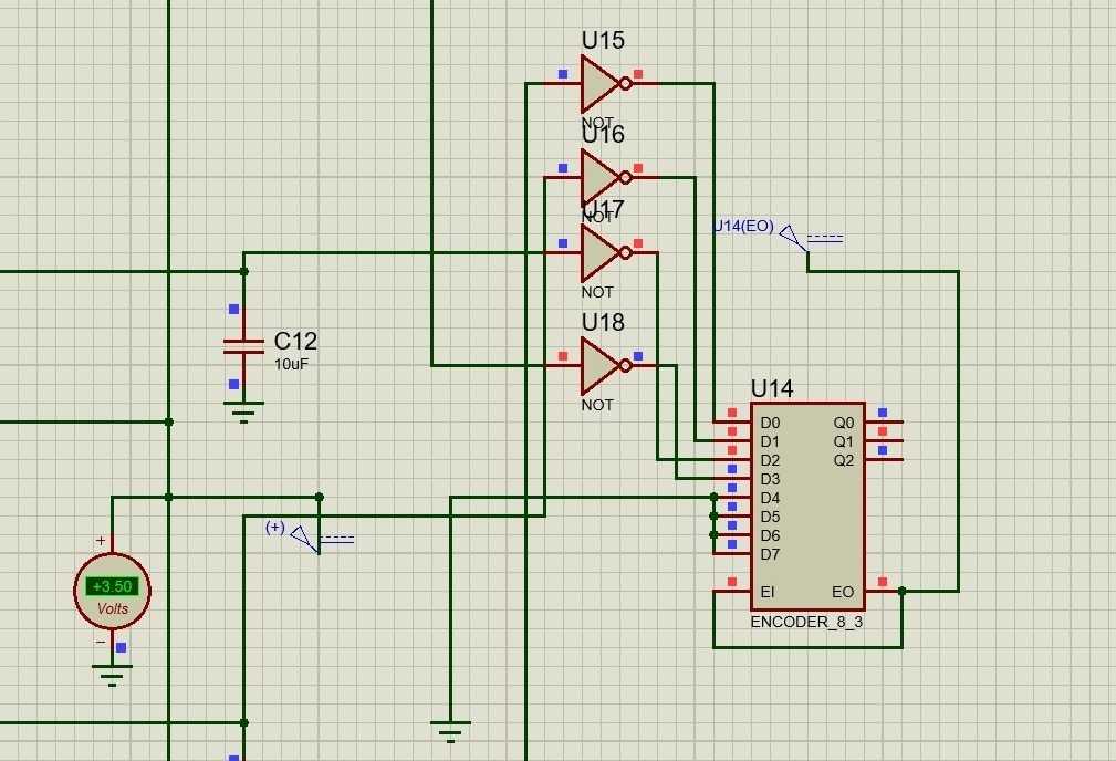
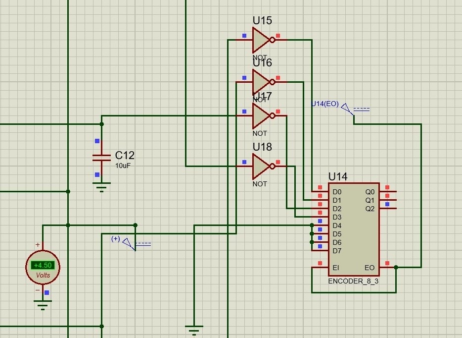
Simulation Output:
| Vin | Encoder Output |
| >1V | 00 |
| >2V | 01 |
| >3V | 10 |
| >4V | 11 |
Red Dot - Logic 1
Blue Dot - Logic 0

Vin>1V, Encoder Output - 00

Vin>2.5V, Encoder Output - 01

Vin>3V, Encoder Output - 10

Vin>4V, Encoder Output - 11
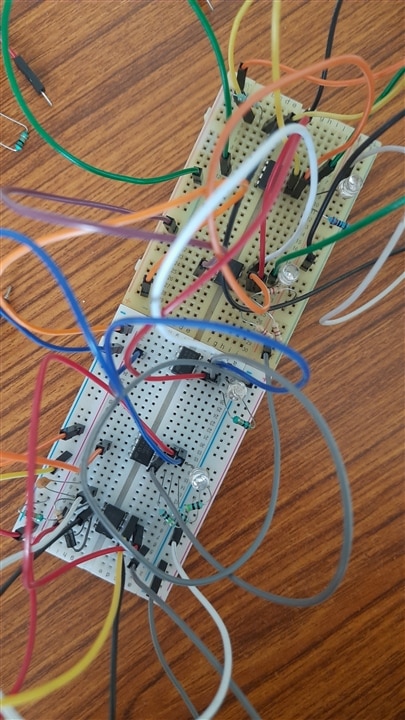
Building this on a breadboard:
I used all of my jumper wires to build this. Evidently, it didn't operate exactly as it had in the simulation. The fanout of my PWM generating IC may be ignored, and as a result, it may not be able to drive all four of my ICs, as I suspect.
I appreciate you reading this far.
This was my first design challenge, as well as the first blog I ever wrote. Please rate my circuit and tell me how to make it work in reality, as well as let me know if there are any improvements I should make on my end.

For me, the task was a 555 MADNESS in every way.
