
In this blog post I will describe my project which I have done as part of Project14 | Build Projects Using 7-Segment Displays! Competition. This project I implemented for testing possibility of adjusting output voltage of step-down voltage regulator using DAC. I successfully completed it. After completing I get DIY dual channel digitally adjustable and controllable power supply.
See it in action!
You can see my power supply on following video:
Sample Sponsors
I would like to thank Maxim Integrated (now ADI) for sending free samples of chips which I have used in this project. Maxim Integrated sent me their MAXESSENTIAL01 Essential Analog Toolkit containing MAX5715 DAC which I have used in this project, and they also sent me MAX16935 Automotive Stepdown regulators and few other chips. All these I received for free.

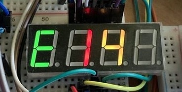
Dual (triple) color 7-segment display
In project I used dual color 7-segment display. It has green and red LEDs in all channels and digits. When you turn both LEDs on then you get yellow color. By adjusting timing, you can also achieve more colors, but you can’t get blue color using this dual color 7-segment LED display.
Block diagram

Pinout
Components are connected to the following NUCLEO (NUCLEO-L552ZE-Q) board pins. All pins are exposed on CN7, CN8, CN9 and CN10 which are presoldered by default. You do not need to use CN11 and CN12 (which are not placed by default).
4 digit dual color 7-segment display (DISPA)
Display is internally connected as follows (screenshot from datasheet).

Pinout to NUCLEO board is following:
- PD0 - DISPA_A
- PD1 - DISPA_B
- PD2 - DISPA_C
- PD3 - DISPA_D
- PD4 - DISPA_E
- PD5 - DISPA_F
- PD6 - DISPA_G
- PD7 - DISPA_DP
- PB0 - DISPA_GREEN_1
- PB1 - DISPA_GREEN_2
- PB2 - DISPA_GREEN_3
- PC3 - DISPA_GREEN_4
- PB4 - DISPA_RED_1
- PE2 - DISPA_RED_2
- PB6 - DISPA_RED_3
- PC0 - DISPA_RED_4
Alphanumerical display (DISPB)

Alphanumerical display shares pins with previously mentioned display but connect more wires to port D. Note that I did not connect channels K, M, S and R because I did not need them. Because display brightness were low, I switched its power by transistor rather directly powering it from MCU. For similar reason, I dedicated two multiplexer clock cycles to him for increasing brightness.
- PD0 - DISPB_A
- PD1 - DISPB_B
- PD2 - DISPB_H
- PD3 - DISPB_N
- PD4 - DISPB_C
- PD5 - DISPB_U
- PD6 - DISPB_P
- PD7 - DISPB_G
- PD8 - DISPB_T
- PD9 - DISPB_D
- PD11 - DISPB_F
- PD12 - DISPB_E
- PC1 - DISPB_YELLOW_1
Buttons
Buttons are connected using pull-up resistor and wired to following pins of MCU:
- PE14 - BTN0 (Channel 1 select)
- PE15 - BTN1 (Channel 2 select)
- PB10 - BTN2 (Start/Stop)
- PB11 - BTN3 (Start/Stop all)
Status LEDs
Status LEDs are connected to the following pins:
- PG1 - LED1_BLUE
- PG0 - LED2_BLUE
- PE3 - STS_LED1_GREEN_1
- PE6 - STS_LED1_RED_1
- PF0 - STS_LED2_GREEN
- PF1 - STS_LED2_RED
Potentiometer
Potentiometer is connected to 8th ADC1 channel – It is connected to pin PA3.
MAX5715 DAC
DAC is connected using SPI bus to the MCU. Clear signal is pulled directly high. I used my breakout:

Connection to the MCU is following:
- PA4 – CSB
- PA5 – SCLK
- PA7 – DIN
- NC – RDY
- NC – LDAC
Outputs from channel A and B are connected to the feedback pin of MAX16935 Step-down regulators.
MAX40080 CSA
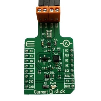
I used MikroE Current 6 Click Board from Experimenting with Current Sense Amplifiers. Connection of pins is following:
- PB8 – SCL
- PB9 – SDA
- PC6 – EN
- NC – ALR
INA219 CSA
Because I have only one MAX40080 CSA, I ordered breakout of second CSA. For gaining experiences with more CSAs, I ordered cheap INA219 Breakout from Aliexpress. Connection is following:
- PF14 – SCL
- PF15 – SDA
MAX16935 Step-down regulators
The last part is the most important part. Step-down voltage regulators. I designed my own board for using this regulator. Board is designed as a standalone (non-digitaly adjustable) board. Output voltage of board can be set by potentiometer. Board looks as follows:
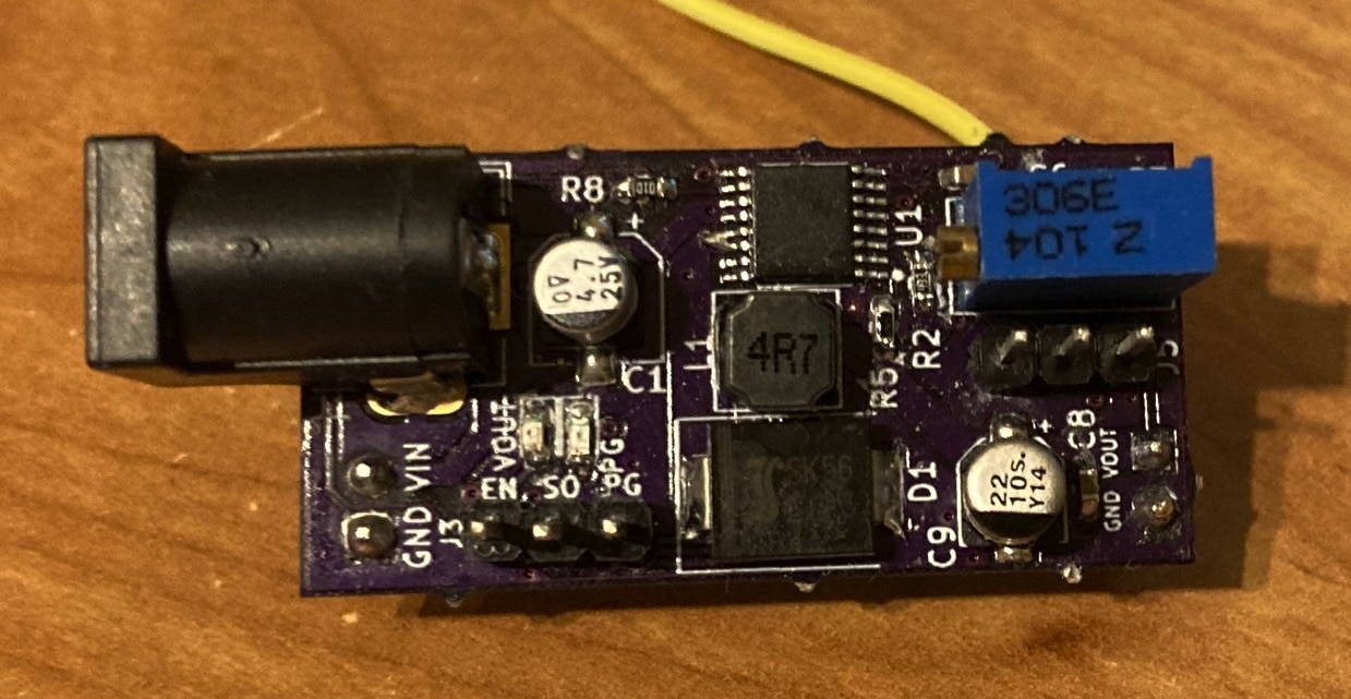
And back side:

The yellow cable is “patch” for exposing feedback pin. I build two units of these regulators, so I was able to make dual channel power supply.
Schematics of the board is following (you can download it in PDF at the end of blog post):
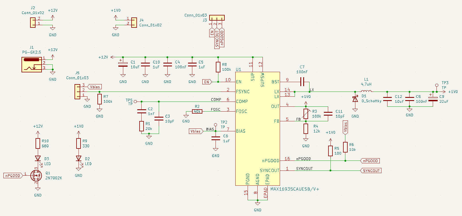
Note that there are mistakes related to onboard LEDs. Both LEDs should be driven by transistor, LEDs resistor should be higher (10k – 45k) for my RED LED. At last, PCB silkscreen labels next to LEDs are swapped (diode with label PG is in fact powered from output, and voltage marked as VOUT is controlled by nPGOOD signal). Otherwise, board looks correct and works. At load regulator drops a lot of voltage. This is most probably caused by some transitive resistance on contacts. My soldering skills are pretty bad. I also used alternative values in case of components which I do not own.
These regulator boards I connected to my digitally adjustable PSU. Regulator feedback pin is connected over 34k resistor to the DAC (channels A for first regulator and channel B for second regulator). Last thing which I used was enable pin. I want to enable and disable regulators form MCU, so I utilized EN pin which is exposed on pinhead on the boards. Little issue is that enable pin voltage levels are related to input voltage (12V), so I was unable to drive them directly from MCU and I had to use NMOS transistor for switching them:

DC/DC output voltage digital adjustment
Now I will describe how does digital adjustment of output voltage works because this is the most interesting part on this project (except using dual color segment display of course ). Main source of theory for following description come from resources [1] and [2] mentioned at the end of this blog post.
Almost every adjustable voltage regulator use feedback, (internal) voltage reference and error amplifier or comparators. Regulation works in a way that regulator adjust output voltage to maintain voltage on feedback equal to internal reference voltage. Internal reference is about 0.5 – 1.2V usually. In case of MAX16935 which I have used It is exactly 1V. More frequently I see references 0.8V, but in fact it is not very important. The simplest use case is wiring output of regulator directly to feedback pin. In this case regulator will regulate output to the same voltage as internal reference which is 1V:

But you do not need to connect output voltage directly. Most common usage is with voltage divider. Imagine following connection:
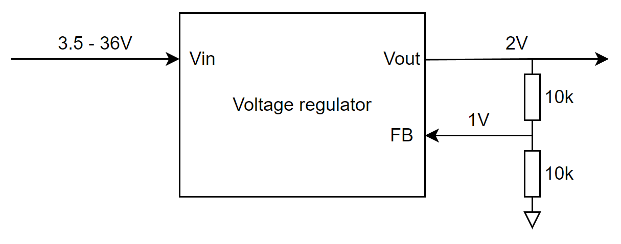
In this case voltage divider is trivial. Because resistors are the same value, half the voltage drops on upper resistor and second half drops on bottom resistor. In the middle you get half of voltage of the top. In this case voltage regulator still operates in the same way – It regulates output for getting 1V on feedback pin (middle of resistor voltage divider). This happens when voltage of output is twice the 1V which is 2V. You can make whatever voltage you want (it must be lower than input voltage, higher than reference and within regulator allowed range) by just changing resistor values of voltage divider. For example, for making 5V, you can choose 40k and 10k resistors:

On my MAX16935 board I replaced upper resistor by potentiometer. So, I was able to adjust output voltage using potentiometer:

And now let’s think of the possibilities changing output voltage of this regulator by some digital circuit. For example, Arduino or some other MCU. The goal is to be able to adjust output voltage of regulator by some digitally driven circuit. Tutorial [1] from Maxim Integrated mention multiple options. Most simple option is replacing mechanical potentiometer by digital one. Digital potentiometer is chip usually bundled with serial interface like SPI or I2C which act as potentiometer, but instead of rotating some mechanical parts, you set level of rotation using this digital interface. Solution with digital potentiometer is easy but digital potentiometers have limited number of steps and digital potentiometers with high number of steps are expensive.
There is other solution. To the middle of divider, we can connect some other (digitally adjustable) voltage source independent on output voltage of regulator.
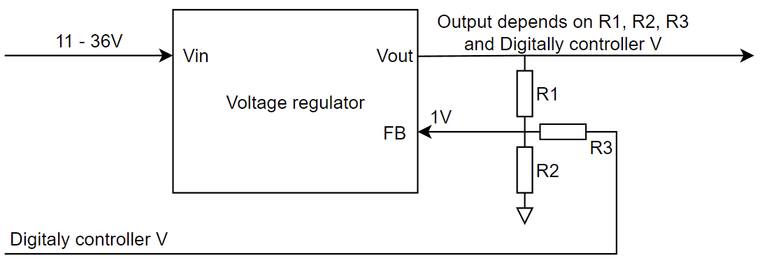
Calculation of divider gets more complicated. Before we start computing dependency between reference voltage, output voltage, adjustable voltage and resistor values, lets think about source of adjustable voltage. The easiest source of adjustable voltage in digital system is DAC (Digital-to-Analog converter). Interface is reverse in comparison with ADC which converts analog signal to digital code. DAC converts digital code to analog signal. The benefit of using DAC instead of digital potentiometer is that it has better resolution and has acceptable price at high resolution. The limit of DAC is amount of sourced/sunk current. In this use case this is not the issue because we can limit current flowing from or to DAC by resistors to acceptable level. We just need use resistors with high enough values.
In this project I used 12-bit MAX5715 DAC which I received for free as an engineering sample from Maxim. Note that most digital potentiometers have 8-bit codes, so DAC solution achieve 16× (2^(12 - 8)) better resolution which will result to more precise regulation of output. This DAC has internal selectable references. I used 4.096V. Note this is voltage of DAC and not the limit of output voltage. Limits of output voltage are defined by resistor values as you will see later. Requirement is that DAC must be able to generate voltages both below and above internal reference of regulator (1V). With DAC able to generate voltage between 0 and 4.096V we easily satisfy this requirement (0V < 1V < 4.096V) and as a consequence we can drive the regulator above and below reference voltage of regulator. Note that with simple voltage divider you never can generate voltage less than internal reference of regulator. With DAC you can do this.
Now, lets compute values of resistors for getting full range of supported output voltages. In project I decided to support voltages in range 1 – 10V which is official supported range by MAX16935 Step-down converter.
Main formula of voltage divider come from Kirchhoff's circuit laws. Idea is that we define directions of current flowing through our resistor divider and apply rule that sum of currents incoming to the junction is equal to sum of currents outcoming form the junction. Direction of currents is not very important. In fact, direction of current flowing to and from DAC will change depending on settings. It is not problem. So, lets intuitively assume current directions in this way:
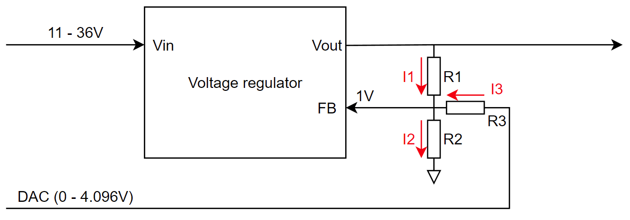
Now we can construct formula using Kirchhoff’s law:

But of course we don’t worry about current flowing through our resistor divider much, so now we replace all currents by voltages and resistors using ohm law.
The easiest is current I2. We know that voltage on upper side of R2 is reference Voltage which is 1V in case of MAX16935. Bottom side is connected to groud, so voltage drop on this resistor is 1V. From ohm law U = R * I which is equivalent to I = U / R we can express I2 as:

Current I1 can be expressed using similar formula, but now voltage drop is different. Now it is not referenced to ground but it is referenced to feedback voltage (1V). So, voltage drop is expressed as difference of these two voltages:

And current flowing through resistor R1 can be expressed as:

Finally similar rule applies for resistor R3. Voltage drop is now difference of feedback voltage and voltage set by DAC.

Now we can assign current expressions to first formula:

This formula you can also find in literature [2]. For simplification I will replace occurrences of Uref by 1V which is reference voltage used by my MAX16935:

Now we need to determine values of 3 resistors for being able to regulate circuit over whole range in which we can regulate. You can do following calculation for whatever range you want. If you for example want to regulate voltage output in rage 3V to 4V, you can simply use these number. I will calculate resistor values for whole supported range by MAX16935 which is 1 to 10V.
The purpose of calculation is that I we need to state corresponding desired output for two boundarueis of Udac – for maximum possible value of Udac (4.096V, I will use 4V for simplicity) and minimum possible value of Udac which is 0V. When we increase DAC voltage, output voltage decreases and vice versa. This is because when we increase voltage, regulator sense that output is higher than it should be and reduces output voltage. Similarly when we set voltage lower voltage than reference regulator will increase output voltage until it achieves reference voltage on feedback pin. So when we regulate DAC to minimum voltage 0V we want to see 10V on output and when we set DAC to 4V we want to see 1V on output. Lets’ fix this value in previous formula. We get two new formulas handling both cases:
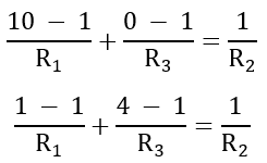
After simplification of calculations:

After removing zero expressions:
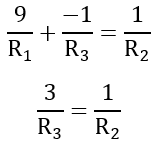
Now you need to select value of one resistor. I chosen R2 as starting point because I soldered fixed 12k resistor here. So, lets assume R2 is 12k. If we get some uncomfortable value like very large or very small value of other resistor, we can return here and try different value.

From second equation we can directly compute value of resistor R3:
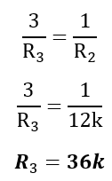
And finally, we can use first equation for computing last resistor R1:

Instead of R1 I am using potentiometer, so I set this potentiometer to 81k.
So, for summarize. If I set R1 to 81k, R2 to 12k and R3 to 36k, I will be able to regulate voltage in full range between 1 and 10V using DAC.
Exactly these settings I used in my project. The last thing which remained unanswered is how to compute what code we have to set for getting target voltage. For example, imagine you want to get 5V on output. What voltage do you have to set on DAC? Answer is hidden in this formula which you have already seen above:

Now Uref, R1, R2 and R3 are known constants which we can assign, but for illustrative purposes I will assign only Uref now:

And now you can assign resistor values for getting final formula:

So, for example for getting 5V on output you need to set DAC to:

2.222V corresponds to code 2222 on 12-bit DAC (4096 possible values) and 4.096V reference.
Formula shown above is used in my firmware if no calibration data are present.
MCU Firmware
MCU firmware is responsible for controlling all peripherals and handling possible errors of these components. MCU firmware is written in C. I developed firmware for SMT32L552ZE MCU using STM32CubeIDE and I used available code generator. I based my firmware on FreeRTOS. There are 13 threads handling peripherals communication and state machine. RTOS interleave their execution on Arm Cortex-M33 CPU core. Threads are responsible for:
- Default thread generated by STM32CubeIDE
- Thread responsible for configuring and retrieving samples from MAX40080 CSA
- Thread responsible for configuring and retrieving samples from INA219 CSA
- Thread responsible for detecting button #1 (select ch1) press, long press and debouncing.
- Thread responsible for detecting button #2 (select ch2) press, long press and debouncing.
- Thread responsible for detecting button #3 (start/stop) press, long press and debouncing.
- Thread responsible for detecting button #4 (start/stop all) press, long press and debouncing.
- Thread responsible for managing color and blinking of RED/GREEN status led #1
- Thread responsible for managing color and blinking of RED/GREEN status led #2
- Thread for enabling, disabling, setting output voltage and monitoring operation of ch1
- Thread for enabling, disabling, setting output voltage and monitoring operation of ch2
- Thread for managing user interface (showing data on displays, triggering operations in other threads and so on).
- Thread for triggering ADC conversion and reading potentiometer status.
As you can see there is no thread for controlling 7-segment display. For achieving better and more accurate timing of switching LEDs, I use HW timer and interrupt handler. Configuration of display digits and channel is static but easily extendable. For example, adding another digit is trivial task requiring only connecting segments to port D, defining select channel GPIO and polarity of select signal.
For assuring thread safety when triggering operations between threads I use 11 mutexes.
For controlling MCU peripherals I use STM32L5 HAL Library provided by ST. For controlling MAX5715 DAC I use my own mini library implemented as part of this project. For controlling MAX40080 CSA I use my own library which I implemented as part of Experimenting with Current Sense Amplifiers Contest. For controlling INA219 I wrote minimalistic library as part of this project. Lastly, I wrote my minilibrary for debugging outputs on UART. So except STM32L5 HAL library and FreeRTOS all other code is my own.
Summary
This is all from this blog post showing my project. I spend last two weeks with implementing it. It was so many wires on breadboard but after connecting all of them it worked well. I successfully utilized multicolor segment display, learn and understood theory about digital adjustment of voltage regulator, implemented it and was fascinated by it . I also improved my skills with STM32 environment and debugging FreeRTOS application and deadlocks. I soldered three boards (MAX5715 Breakout and 2x MAX16395 Step-down Voltage Regulator) and connected about 50 wires on breadboard. I welcome any feedback regarding my project, so feel free to comment below.
Resources
- MAX5715 Breakout Schematics (PDF)
- MAX5715 Breakout Gerbers (ZIP)
- MAX5715 Breakout Kicad Project (ZIP)
- MAX16935 Step-Down Regulator Board Schematics (PDF) (note the mistakes mentioned above!)
- MAX16935 Step-Down Regulator Board Gerbers (ZIP) (note the mistakes mentioned above!)
- MAX16935 Step-Down Regulator Board Kicad Project (ZIP) (note the mistakes mentioned above!)
- MAX40080 CSA C Library (Github)
- Firmware source codes (ZIP)
- Prebuild firmware image (ELF)
References
I gained my knowledge in these two articles:
