The following example of 7 segment display is implemented in an FPGA by hardware/software co-design. The video shows that the system has an ascend/descent control and reset button.
Video demo of the co-design function
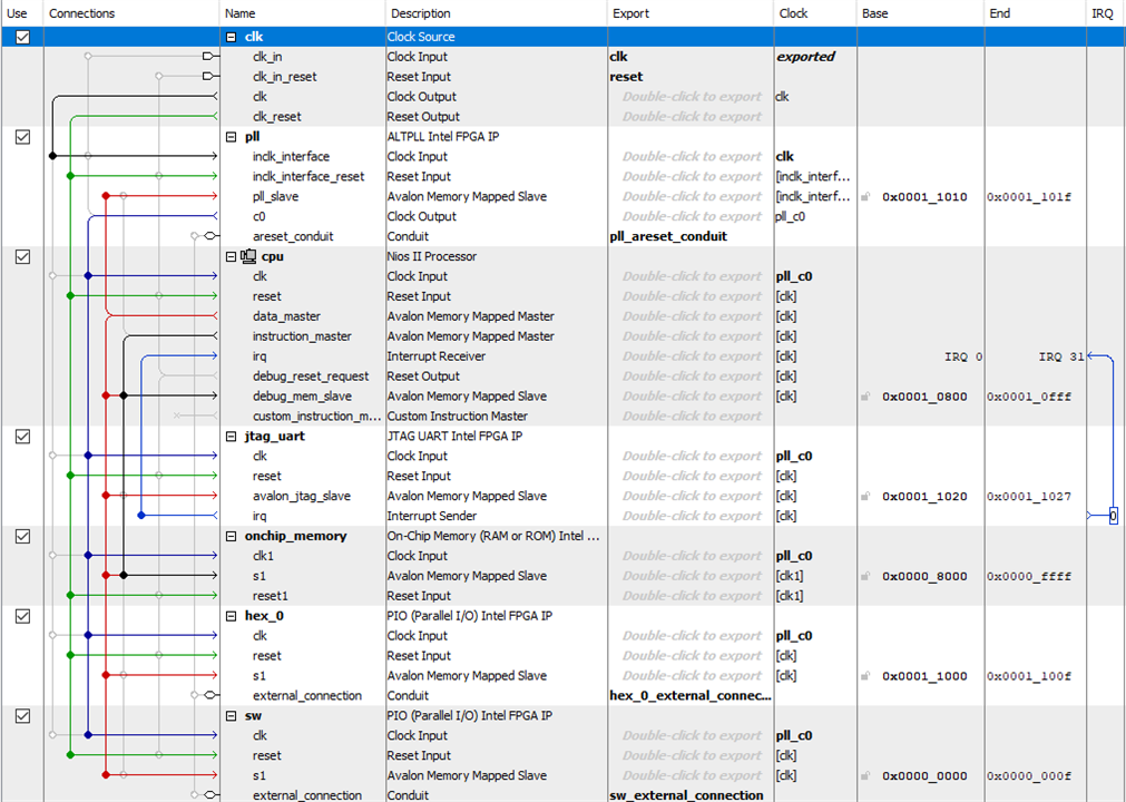
How is this achieved? There are two designs: architecture and software. The architecture, shown below, consists of two Parallel Input Output (PIO) peripherals. One of these peripherals is mapped to 7 segment displays, in this case, with dot point. The other one is mapped to a switches group to acquire external information to control the direction of counting.

Architecure implemented. It consist of NiosII/e, on-chip RAM Memory with 32768 bytes, JTAG interface for debug and programming, and two PIO instances.
The board used is a STEP FPGA MAX 10 with a 10MSAM08 device. This device has 8K Logic Elements (LE), 378Kb of M9K Memory, sufficient to instantiate a Nios II/e processor and the peripherals for this work. In addition, a PLL is needed to meet clock requirements for a JTAG instance because the clock available has a 12MHz oscillation. Finally, the on-chip memory for instruction storage has 32768 bytes. This configuration requires 21% of available logic elements and 71% of memory.
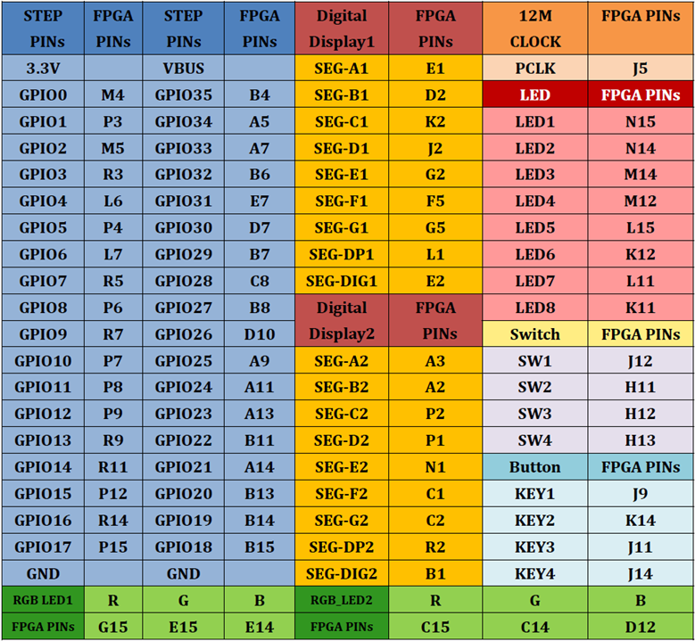
According to the STEP FPGA Hardware Manual, the pin assignment for each device is the following,

STEP FPGA pin Assignment. The implemented logic is positive
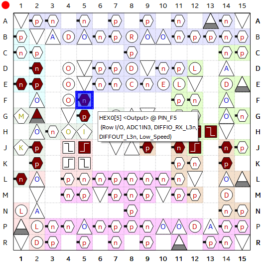
Only the 12M clock, Switch, and Digital Display 1 assignments are required here. The 12MHz is the clock source for the PLL and a 50MHz clock source is generated. It is possible to use the Pin Planner interface to create interactively the device mapping. Another form to do device mapping is with the Assignment Editor or by a .qsf file. In addition, a button must be mapped to reset the system.

Pin Planner with device mapping. Only 16% of pins are required for this implementation
To create the co-design, the architecture must be instantiated and mapped according to the pin assignments, consequently, a small HDL file is required to compile the Hardware, map, and create the Application with its Board Support Package (BSP).
library IEEE;
use IEEE.STD_LOGIC_1164.ALL;

entity step_nios is
	port(	PCLK	: in	std_logic;
			KEY	: in	std_logic_vector(3 downto 0);
			SW		: in	std_logic_vector(3 downto 0);
			HEX0	: out	std_logic_vector(8 downto 0));
end step_nios;

architecture arch_interface of step_nios is

	component base_arch is
		port (
			clk_clk                          : in	std_logic                    := '0';
			hex_0_external_connection_export : out std_logic_vector(8 downto 0);
			pll_areset_conduit_export        : in  std_logic                    := '0';
			reset_reset_n                    : in  std_logic                    := '0';
			sw_external_connection_export    : in  std_logic_vector(3 downto 0) := (others => '0')
		);
	end component base_arch;

begin

	u0: base_arch
		port map(
			clk_clk									=> PCLK,
			hex_0_external_connection_export => HEX0,
			reset_reset_n                    => KEY(0),
			sw_external_connection_export    => SW
		);

end arch_interface;
On the software side, the C bare metal base code to control the display and direction takes the base address of peripherals to read and write data.
#include <stdint.h>
#include <unistd.h>
#include "system.h"

uint32_t codes[10] =	{	0b010111111,//0
							0b000000110,//1
							0b011011011,//2
							0b001001111,//3
							0b011100110,//4
							0b001101101,//5
							0b011111101,//6
							0b000000111,//7
							0b011111111,//8
							0b001101111//9
						};

int main(void){
	uint32_t *hex0 = (uint32_t*)HEX_0_BASE;
	uint32_t *sw = (uint32_t*)SW_BASE;
	int8_t i = 0;
	uint32_t input = 0;
	while (1){
		*hex0 = codes[i];
		input = *sw & 0x0001;
		if(1 == input){
			i++;
		}else{
			i--;
		}
		if(i >= (int8_t)(sizeof(codes)/sizeof(codes[0]))){
			i = 0;
		}else if(i < 0){
			i = sizeof(codes)/sizeof(codes[0]) - 1;
		}
		usleep(250000);
	}
	return 0;
}