


Why I Built It
The project that eventually became SillyScope started because I wanted to learn how to make my own PCBs for my university rocket team. The basic idea was essentially to make my own “homebrew Teensy”, using a custom STM32 board that I could design, route, manufacture, assemble, program, and bring up entirely myself.
The first version of this custom PCB, Biggy Rev 0.1, was intentionally kept relatively simple. The main goal was not to pack it with features, but to prove that I could successfully build a six-layer board around the STM32H573IIT3Q and get it working. It gave me experience with BGA fanout, power distribution, USB, programming/debugging, multilayer PCB layout, hand assembly, and hardware bring-up. Rev 0.1 ended up as a 63 × 65 mm board and most importantly, it worked.
The idea for turning Biggy into an oscilloscope started before it ever physically existed. I had heard of the Show and Tell competition and was excited that I now had a real reason, not just for learning, that I could use Biggy for. I chose an oscilloscope for my project because it would push me to squeeze out every bit of performance from this MCU as I possibly could.
The Working Scope
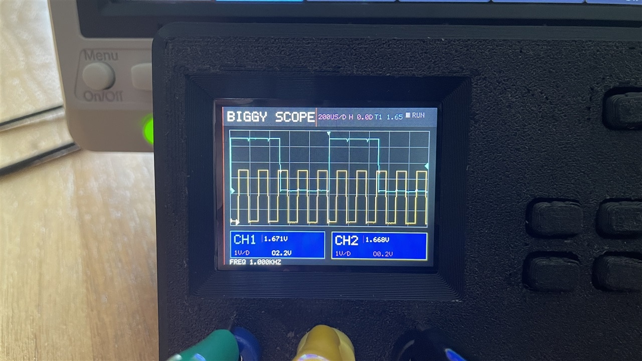
Biggy has now reached the point where it works as a real two-channel oscilloscope. Both channels can be displayed at the same time, with independent voltage scaling and vertical positioning, while the time base and horizontal position control the overall view. The scope also includes adjustable triggering with selectable source, level, and rising or falling edge, along with voltage and frequency measurements and a RUN/STOP function for freezing a capture.
Getting the scope to this point involved a lot of firmware iteration, especially around keeping the waveform stable while continuously sampling and updating the display. The photo above shows both channels running together, with CH1 in blue and CH2 in yellow, while measuring a 1 kHz and 5 kHz signal. It is still very much a homemade instrument, but it has progressed far beyond simply plotting ADC values on a screen.
How the Signal Gets to the Screen
Each input is sampled by its own ADC inside the STM32, with a hardware timer keeping the two channels synchronized. Instead of having the CPU constantly read every ADC conversion, circular DMA (Direct Memory Access) continuously transfers the samples into memory. The buffer is divided so that DMA can keep filling one section while the firmware works with previously captured samples. From there, the STM32 finds the selected trigger point, converts the ADC values into screen coordinates, and draws the grid and waveforms into a framebuffer.
The display has its own DMA pipeline, so the CPU does not have to manually transmit every pixel either. I originally tried running the entire ST7789 interface at 64 MHz to get the fastest possible refresh rate, but this caused glitches in parts of the UI that were updated less often, such as text, measurements, and other smaller screen elements. The final solution was to run commands and smaller updates at a more reliable 32 MHz, then switch up to 64 MHz for the large framebuffer transfers. This kept the waveform updates fast while avoiding the display corruption I was seeing before. At the same time, the ADCs can already be collecting the next samples while the CPU processes the current capture and DMA moves the previous frame onto the display.
The Parts That Pushed Back
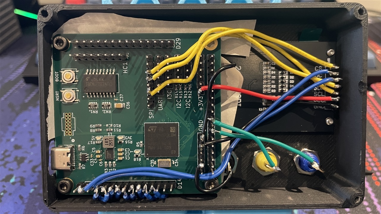
Surprisingly, the hardware itself did not give me many problems. The only mistake was the pushbutton footprint. I had accidentally placed GND and the NRST/BOOT signals on the same internally connected side of the switch, so as soon as the buttons were installed, those nets were shorted together. Luckily it did not require a PCB revision, so I simply cut off two opposing legs so that only the contacts I actually needed were connected.
The firmware was where most of the fighting happened. Early versions of the scope only managed a few frames per second, faster timebases could become choppy or completely freeze, and getting the trigger to consistently lock onto a waveform took a lot of experimentation. I also pushed the display too far by initially running everything at 64 MHz, which caused glitches in UI elements that updated less frequently. That eventually led to the current 32 MHz / 64 MHz display system.
I also experimented with a faster “turbo” acquisition mode that used both internal ADCs together on a single channel. It looked promising but ultimately caused the waveform to freeze and had to be backed out. Most of the development became a cycle of increasing the performance, finding whatever broke next, and then rewriting that part of the firmware until it behaved.
Checking It Against My Siglent SDS 1202X-E
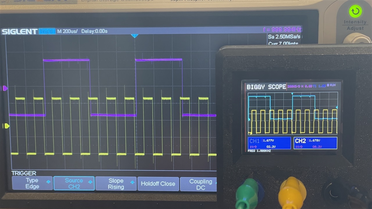
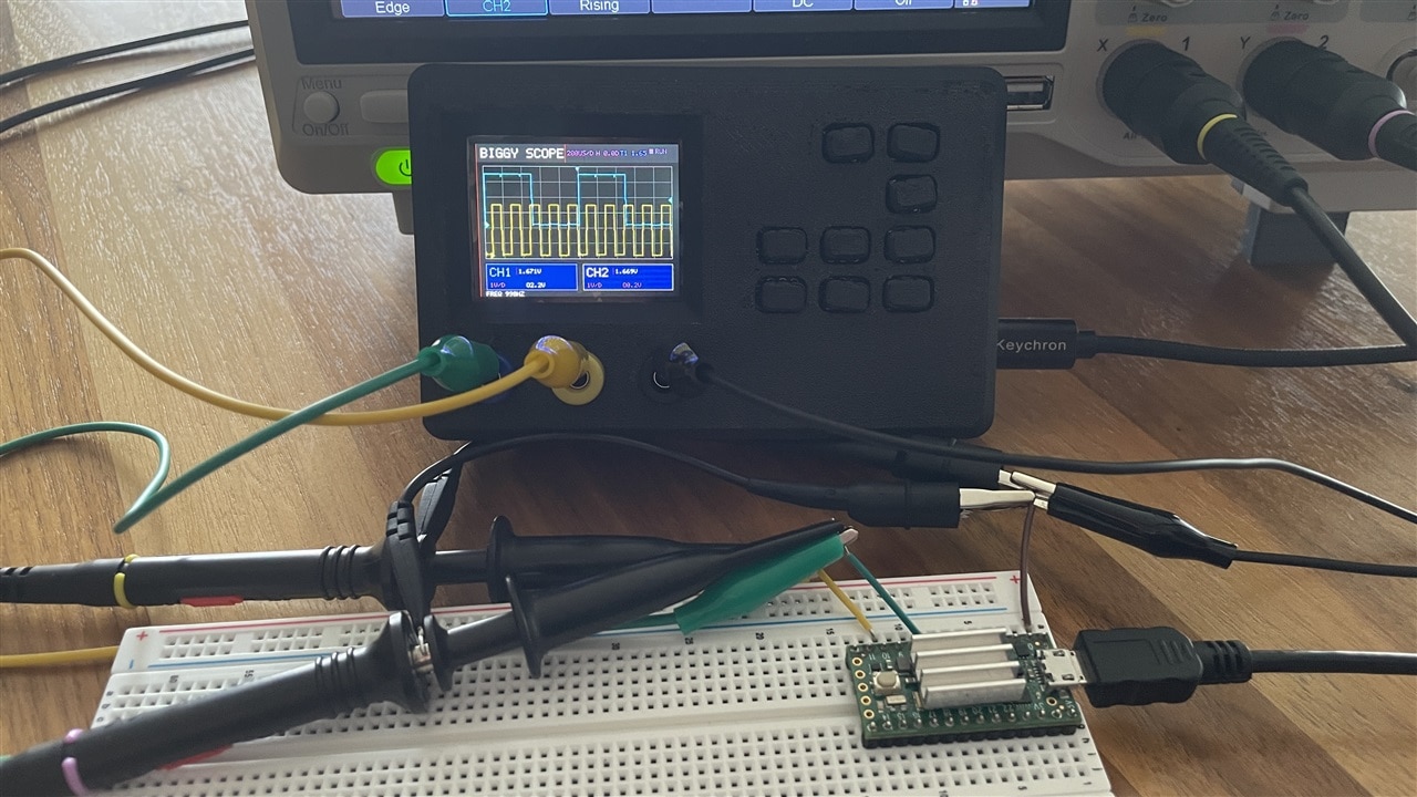
To check how SillyScope compared with a real instrument, I generated 1 kHz and 5 kHz square waves from a Teensy and measured the same signals with both SillyScope and my Siglent bench oscilloscope. The timing and waveform shapes lined up closely between the two, and SillyScope measured the 1 kHz signal at 1.000 kHz while the Siglent read about 999.994 Hz. Seeing the homemade scope reproduce the same signals beside a commercial bench scope was a pretty satisfying confirmation that the acquisition, triggering, and display system were working properly.
From Prototype to the Next PCB
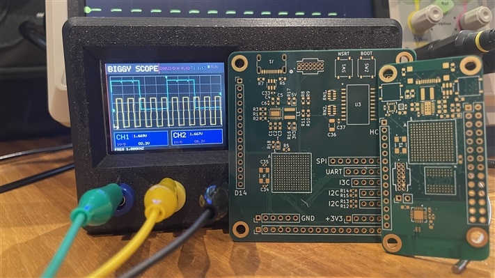
Biggy Rev 0.1 proved that I could design, assemble, and bring up a custom STM32 board, so Rev 1.0 was about seeing how far I could push that idea. The new board was made much smaller and significantly denser while adding external SDRAM, microSD storage, wireless communication, sensors, improved power circuitry, and a much more refined overall layout. It also pushed me into more advanced PCB design techniques such as tighter BGA fanout, via-in-pad, RF layout, dense multilayer routing, and much more careful placement and power distribution. Rev 0.1 was the proof that the idea worked; Rev 1.0 (photo below) was the first design where Biggy started to look like a genuinely capable embedded platform rather than just a development board.

What I Learned
Biggy taught me far more than just how to make a working PCB. I learned how to design around a large BGA MCU, route a multilayer board, manage power and grounding, bring up hardware, debug mistakes, and write firmware that makes heavy use of timers, ADCs, DMA, triggering, and high-speed display transfers. It also taught me how much iteration matters—many of the biggest improvements came from repeatedly testing something, finding its limit, and then redesigning that part of the system.
The biggest difference, though, is probably how much better I have become at PCB layout. Looking at Biggy Rev 0.1 beside Biggy Rev 1.0 makes that pretty obvious. Rev 0.1 was much more spread out and routing was mostly about simply getting every connection where it needed to go. Rev 1.0 is dramatically denser, more organized, and much more deliberate about placement, routing, power distribution, RF, and overall board structure. More than anything else, Biggy gave me the confidence to take on much more complicated PCB designs than I would have attempted when I started.
Rev 0.1

Rev 1.0

Top Comments