


Badge
Table of Contents
- What is this project all about?
1.1 The project in one paragraph
1.2 Why I started this project instead of buying a finished product
1.3 Current status in the overall project plan - Design goals and constraints
2.1 Requirements
2.2 Why E-Paper technology
2.3 Formfactor
2.4 Why choosing a bare ESP chip over a prebuilt module - System architecture
3.1 Overview over all sections
3.2 Power input system and fuel gauge
3.3 Buck/boost systems
3.4 MCU section
3.5 LED driver
3.6 E-Paper driver
3.7 Upcoming systems - PCB design
4.1 Layout approach and floorplanning
4.2 Silkscreen
4.3 Board revision 1.0 to 1.1
4.4 The assembly process - Housing
- What went wrong, which challenges did I face and how did I solve them?
6.1 USB not enumerating
6.2 ESP32-S3 alignment on the PCB
6.3 Unstable 3.3V rail caused by contamination
6.4 Charger circuit seemed to not charge the battery
6.5 E-Paper suddenly not responding in rev 1.1
6.6 Troubleshooting and challenges conclusion - Firmware
7.1 Toolchain and framework
7.2 Power management and sleep behaviour - Where it stands now
8.1 What works
8.2 What doesn't work yet - Next steps
9.1 My vision of the finished project
9.2 Specific changes in rev 2.0
1. What is this project all about?
1.1 The project in one paragraph
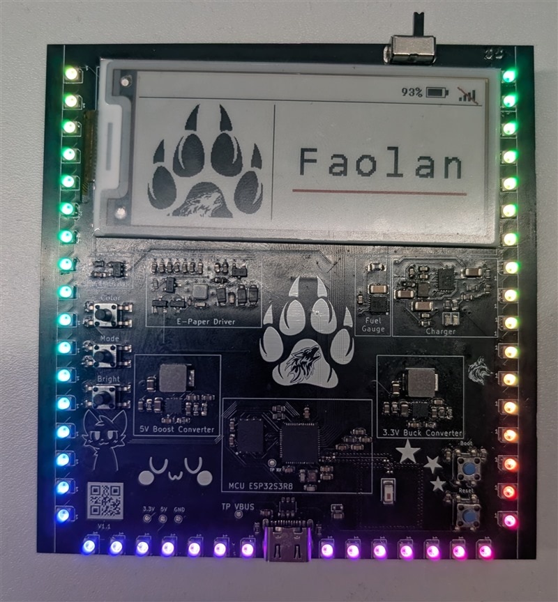
The goal of this project is to have a fancy, wearable name badge for conventions or tech fairs. The badge is based on an ESP32-S3R8 chip with a 4-color E-Ink display and 48 individually controllable LEDs. It also enables the user to change things like the image, icon, theme, size, etc. over a WiFi connection.
1.2 Why I started this project instead of buying a finished product
There are several reasons why I started to design my own badge instead of buying one from the internet. There are a lot of different products out there which everyone can buy for a few bucks, but I think that is not special, nothing where people really come up to you and say how cool they think it is. And even if they do, the only thing you did was spend some time on Amazon or AliExpress. But with this self built badge, that is something you can talk about in conversations and be proud of.
Additionally I do like new and challenging projects, and this overengineered name badge seemed to be the right one to learn a lot of new stuff about PCB design, SMD soldering and working with components you cannot buy as an Arduino compatible breakout board.
1.3 Current status in the overall project plan
The current state of the badge is revision 1.1, which features 48 LEDs and one 4-color E-Ink display to convey information and to draw attention. Behind the scenes a powerful microprocessor is built in to control all of these, while having a lot of wiggle room for future features and firmware updates. There is also a powerful power system which controls and measures the power flow precisely. More on that later.
But while this is already functional and could be the end of the project, I want more features, like NFC, LoRa, GNSS and much more. More about that in chapter 9.
2. Design goals and constraints
2.1 Requirements
This project has several requirements. The first one, of course, is to display a name, which is the core task of a name badge, as even the name implies.
Second of all it should look cool, and what looks cooler than a bunch of individually controllable RGB LEDs?
But in addition to all of that it should still be practical: the battery should hold for a good amount of time, I need to know how much power is left, need to think of what happens if the power runs out in the middle of the day, how long charging takes, how to comfortably wear it, and so on.
2.2 Why E-Paper technology
When thinking about power efficiency and how to display a name without the requirement of having a full battery, an e-paper was the first thing which came to my mind. It can be updated at all times, but if the power goes out it still displays the name like nothing happened, because an e-paper does not rely on power to display its data. That comes from its nature of moving ink particles during refresh cycles, and those particles stay in position even with no power provided.
But there are some real trade-offs, and one of them is the color space: the e-paper I am using has only 4 colors (white, black, red, yellow), and that is already a lot for an e-paper display. Normally they just have two or three colors.
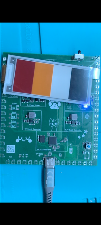
Another trade-off is the refresh time of the display. While most LCD or OLED displays reach refresh rates from 20 frames per second up to 60 frames per second or even more, my e-ink takes about 20s for a single frame. The badge has a small menu for showing battery and WiFi information, but every time I want to navigate in this menu I need to wait 20s until the e-paper is done rendering the frame.
And last but not least, an e-paper has no backlight, which means that as soon as it gets darker outside it is not easily readable anymore.
2.3 Formfactor
It is obvious that there is some limit to the formfactor of the board regarding wearability, but there is also a less obvious factor which had a big impact on the sizing of the PCB. I order my PCBs at JLCPCB and discovered that for a PCB which is exactly 102mm x 102mm I pay around 20€, but if I go just 0.1mm over that limit I instantly pay 30€ more. That is probably because they normally use trays that are exactly 102mm by 102mm, and for everything larger they need to change to larger trays or machines, which is a visible jump in pricing.
2.4 Why choosing a bare ESP chip over a prebuilt module
Normally you would use a prebuilt and pre-certified ESP module like this one:
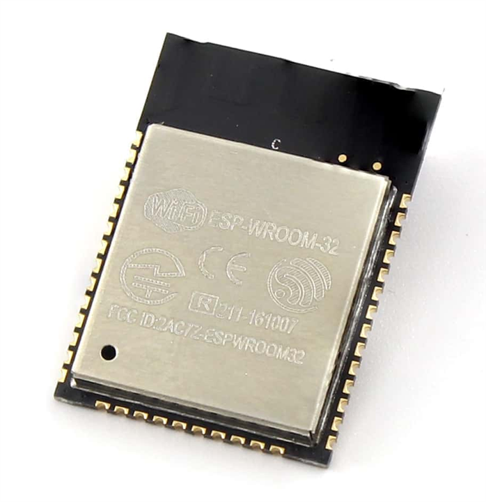
There are almost only advantages in doing it like that:
- Fewer parts to solder
- Cheaper than buying every single part yourself
- You get a properly calibrated antenna
- It is already CE certified, so if you want to sell this as a product it is much cheaper to get an overall CE certificate for the whole design
But I decided against that. Why? There are multiple reasons, and one of them is that I am not doing this as a project I want to finish as cheaply as possible. I want to max out my learning experience while doing it, and soldering the bare ESP chip with all its capacitors and strapping pin configuration taught me much more than using a prebuilt module could ever have done.
Additionally I already own a LiteVNA which I bought for my previous project, and with that I can measure the signal reflection from the antenna and match the impedance with exact and measured values.
And to be honest, I think the pre-certified modules with their metal shield look kind of ugly. There are so many beautiful PCB designs out there based on the ESP32, with nice part placement, nice silkscreen images or text, and then there is a big metal something in one corner sitting on top of the PCB which breaks the overall design. In my design there is nothing like that. The ESP32 is completely integrated into the PCB and therefore creates one consistent style.
3. System architecture
3.1 Overview over all sections
There are 7 important sections on the board, which are also marked and labelled on the silkscreen: charger, fuel gauge, 3.3V buck converter, 5V boost converter, MCU, LED driver and e-paper driver. The chapters below group them slightly differently, because the charger and the fuel gauge sit right next to each other and belong to the same job, and the same goes for the two converters.
3.2 Power input system and fuel gauge
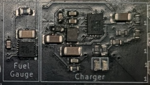
The USB-C port and the battery are directly connected to an MP2617HGL, which charges the battery when a USB-C plug is inserted and powers the system from the battery if no cable is connected. It can switch between both of these power sources seamlessly without any visible power loss for the rest of the system.
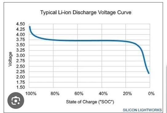
Directly next to it is a MAX17260SETD, a high precision fuel gauge which can precisely measure the remaining percentage of the battery as well as the current that is flowing. This is needed to get a precise remaining battery percentage, because simply calculating it from the voltage via a voltage divider does not work with Li-Ion batteries because of their discharge behaviour.
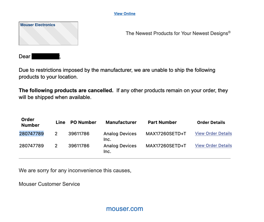
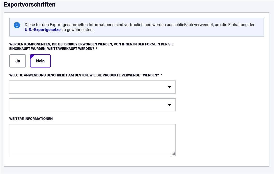
Sourcing the MAX17260 turned out to be the most awkward part of the whole BOM. My order at Mouser was cancelled, with the note that restrictions imposed by the manufacturer meant they could not ship the part to my location. Digi-Key did ship it, but only after I filled in an export compliance form asking whether the components would be resold in the form they were purchased in, and what application they would be used for. I also had to promise that I am not building anything military, aircraft, medical or aerospace related with this component. Not something I expected from a fuel gauge.
3.3 Buck/boost systems
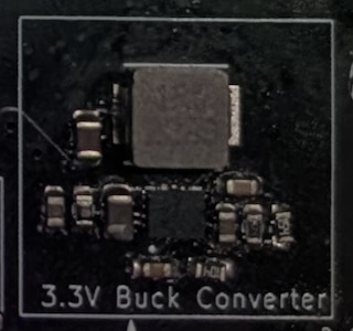
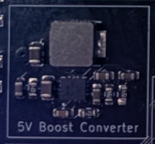
The input voltage for the whole system is not consistent: when USB-C is connected it is 5V, when it is battery powered it is anything between 3V and 4.2V. But the system needs a stable 3.3V and 5V for the MCU and the LEDs.
Therefore I need to step the voltage up and down safely, and that is why I chose the TPS63070RNMR, which can seamlessly switch between boosting and bucking to the selected voltage, configurable with resistors at the setup pin.
3.4 MCU section
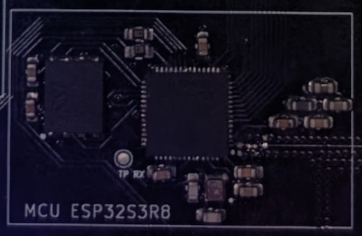
As the microcontroller I used the ESP32-S3R8, which is one of the best ESP32s with integrated WiFi and BLE. In this variant it has 8MB PSRAM but no internal flash, which is why there is a 16MB flash storage chip next to it. That makes it one of the strongest configurations you can easily achieve using the ESP32-S3, with more RAM and storage than most projects would realistically need. But I chose it anyway, because I don't want to be limited by hardware on my own board when new features come along, so I went with the best setup I could easily do.
3.5 LED driver
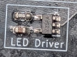
The LED driver is a small level shifter, a 74AHCT1G125W5, which turns the 3.3V signal from the MCU into a 5V signal so the LEDs are more stable when changing color.
3.6 E-Paper driver
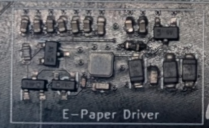
The e-paper driver consists of a boost circuit which generates several rails from the incoming voltage, positive and negative, up to about ±16V. This is required by the e-paper display to get enough voltage to move the small ink particles inside it. The exact rails and the values I measured on them are listed in chapter 6.5.
3.7 Upcoming systems
There are many more sections planned. This will also be discussed in chapter 9, but to mention it quickly, there will be an NFC section, a LoRa section, a co-processor section, a GNSS section as well as a UWB section, which will add massive new possibilities to this board.
4. PCB design
4.1 Layout approach and floorplanning
In the layout approach I always separate the different regions from each other, for the sake of design and for clarity when taking a look at it. Additionally it is worth mentioning that the RF antenna sits in the bottom right corner, far away from any switching logic like the power converters or the LED and display drivers.
The layer layout is quite straightforward: the first layer is data, the second one is ground, which is good for signal integrity, the third is the power plane, where the 3.3V and 5V from the converters go, and the fourth layer is data again.
4.2 Silkscreen
Labelling and outlining every functional block on the silkscreen (charger, fuel gauge, 3.3V buck converter, 5V boost converter, e-paper driver, LED driver, MCU) is a great addition to this PCB. It does not only make it clear what does what, it also helps when debugging, because I can read what a certain section does without having to look into the schematics again.
I also added some pictures and symbols to the silkscreen, which makes the PCB more interesting to look at and makes it a bit more personalized.
4.3 Board revision 1.0 to 1.1
There was also a first PCB revision, and surprisingly it was not replaced because of a technical defect but purely because of a size error: I measured the height of the display wrong, so it didn't fit onto the PCB. That is why in revision 1.1 I moved every component down a little bit to fit the display. Additionally I swapped two GPIO pins with each other for cleaner routing.
Last but not least I removed the NTC sensor from the battery circuit, because I thought this part of the circuit was faulty. In fact it wasn't, which I discovered after ordering the new revision. Additionally I added a new test pad to expose the serial RX more easily for debug reasons.
4.4 The assembly process
The following describes how I assembled rev 1.1. On rev 1.0 the same process did not go quite as smoothly, which is what chapter 6 is about.
For assembling the PCB I put solder paste on all copper pads with the help of a stencil. After that I hand placed every part with tweezers. The size of the parts varied: the buttons, for example, I could place with bare hands, while the components for the antenna circuit had to be placed really carefully because they are only 0.6mm x 0.3mm, which is a real challenge.
After putting all the parts onto the PCB, which took me almost two hours, I put everything on a heat plate and waited for it to be soldered. After that I checked with my multimeter for any shorts, and after confirming there were none I plugged the USB-C cable in and instantly got a connection.
5. Housing
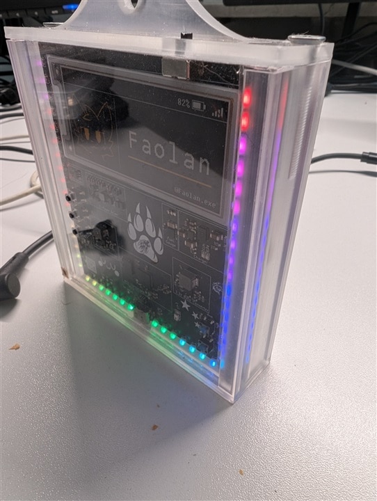
The PCB also needs a nice housing so that you can wear it. It should be solid but should also not obstruct the view onto the PCB. That is why I designed my own: the frame is 3D printed in resin, and the front and back panels are plexiglass, so the board stays visible from all sides.
6. What went wrong, which challenges did I face and how did I solve them?
Even though there was not a single schematic error in my design (which is a crazy fact in itself and not something I expected), and the one part that later caused trouble was a substitution I made while assembling, that doesn't mean I didn't spend hours debugging it. Because of faulty soldering and wrong measurements I still needed around a week to get everything up and running.
6.1 USB not enumerating
This is the first problem I run into on every board I build: I connect it to the computer and hope and pray that it shows up as a USB device in my device list. Of course it did not on the first try.
I searched two full days for the issue. I measured all power rails and the current draw, but everything seemed fine. I reflowed the MCU a dozen times and still got no USB enumeration. I still wasn't convinced that the MCU was sitting correctly, because the 56 pins are spaced around 0.4mm apart, which means being off by just 0.2mm makes either everything or some sides and pins of the MCU stop working.
Since I didn't want to resolder the MCU again, I looked into the USB driver log of my Linux machine. In the past I had problems where only RX was working, so a handshake gets attempted but aborted on timeouts. That is why looking into the driver logs is a good option when the computer recognises the PCB as something, but not as a functional USB device. This time there were no logs at all regarding my PCB.
After that I searched for a way to get any data or logs out of the chip about what it is doing, because the list of possible problems is endless: a faulty clock signal, a short on a power rail, not enough current from the power converters, a misaligned MCU, a problem on the USB lines, a problem with the USB-C port, and so on.
I knew the USB port itself was fine, because I measured the resistance between power and ground with a multimeter and did a continuity test on the data lines and the CC pins using a USB-C cable I cut open.
While searching for what else I could do, I discovered that the ESP does not only have a USB JTAG module to talk to other devices, but also a native serial module that prints out system logs like boot messages. If I can read that, I know exactly what is going on: not booting, wrong clock speed, crashes, and so on. But I also knew that it would not be easy to access, because unlike rev 1.1, rev 1.0 did not have a test pad for that serial pin, so I somehow had to reach the pin directly while the ESP was soldered to the board and running. With a normal cable it would have been impossible to touch a pin that small with no trace going away from it, but then I had an idea: I stripped a cable and wound it around one of my multimeter probes, which has a really pointy tip, and with that I could pick the signal off the pin. I connected that cable and a ground connection to one of my USB to serial converters and started a serial monitor on my laptop. The result: the ESP boots up just fine. Then it reboots because it doesn't find any firmware on the empty flash, but that is fine. That confirmed that everything was working and only the USB data line was faulty.
I thought about resoldering the MCU again, but I didn't really want to, because it is always a hassle and optically it looked connected.
As a next step I tried to narrow down the fault. I looked up the voltage levels a USB connection should have and measured what I actually had. The result: my D+ line was almost 0V, which shouldn't be the case. After bridging the 22Ω resistor I have in series with the data line, the problem still didn't vanish, and I was clueless again.
The next day it struck me: what if the ESD protection, which does not only protect the VBUS line but the data pins as well, is faulty? I desoldered it and bridged the connection with thin copper strands, and the computer connected successfully without any problems.
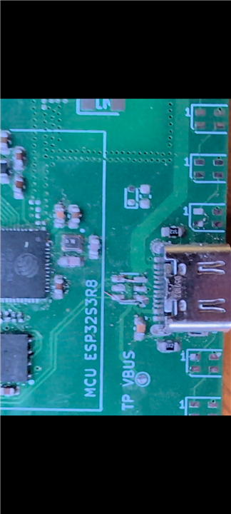
In later builds I used the same part and the same schematic for the ESD protection without any problem, so it was probably either a faulty one or it got damaged by heat during the process.
6.2 ESP32-S3 alignment on the PCB
Like I already mentioned, placing the ESP32-S3 with all of its 56 pins on the PCB without any misalignment is not that easy. I work with hot air on the lowest fan setting, but it is still enough airflow that the chip doesn't align itself through surface tension. This gets worse after a few iterations, when there is a little bit too much old solder paste on the pads.
What helped me the most was placing the MCU and all other components one after another and then putting the whole board on a heat plate. I did it that way for assembling rev 1.1, and the ESP self aligned correctly on the first try. On a half assembled board I didn't want to risk damaging the other components with the heat plate.
6.3 Unstable 3.3V rail caused by contamination
In the first revision I also had the problem that the 3.3V rail did not have 3.3V. It had anything from 1.9V up to 10V. It was really weird behaviour, because sometimes the voltage was stable and stayed that way over a few power cycles, but after reflowing the buck boost chip I sometimes got fluctuating voltage levels instead.
In the end the fix was easy: I desoldered the power IC once again and cleaned it and the PCB with isopropanol, and after that it worked perfectly. I think remaining flux and solder paste allowed really small currents in the µA range to flow, or bridged the two voltage divider resistors and changed them by a few ohms. Normally that wouldn't be a big deal, but the feedback divider pin is quite sensitive to leakage currents like that and to small resistor value changes, and therefore it produced weird output voltages.
6.4 Charger circuit seemed to not charge the battery
After everything else was fixed, so the LEDs worked, the e-paper worked and the USB communication worked, I wanted to find out how much current the charging IC can actually push into my battery. Instead of using the fuel gauge that is already built into the board, I used a multimeter. There were two reasons for that. At first I simply forgot that I had the fuel gauge on the board, and after I remembered it, I didn't trust it. I thought a multimeter would definitely give me the correct value, so I could use that to double check the fuel gauge.
So I put my multimeter in series between the charger IC and the battery. But I only measured around 5 to 20mA, which is nowhere near enough, because it should have been way higher. At least a few hundred mA.
In the process of troubleshooting I removed the NTC sensor and changed a few resistor values to tweak the configuration of the charger IC, but nothing seemed to work. In the end I gave up on it and ordered the next revision, because everything else worked and I wanted the project ready for a specific deadline, since I wanted to take it to a convention. I only removed the NTC sensor in that revision and did not make any more changes, because I could not find any errors in my schematic.
While the next revision was being produced and shipped, I tried out the fuel gauge, and I found something wild: it showed more than 1000mA going into the battery. Same configuration, same charger, same cable as before. I was happy and devastated at the same moment. Happy because it worked, devastated because it had worked all along and I was just too stupid to measure it correctly, because I never thought about the burden voltage my multimeter was producing.
A multimeter measures current by putting a shunt resistor in series with the circuit, and I measured mine at around 10Ω on the mA range (it fluctuated between 9.6Ω and 10.1Ω, so 10Ω is close enough for this calculation). Mine is a cheap 20€ meter from Amazon, so that value will be a lot lower on better equipment, but the effect itself does not go away. That doesn't sound like much, but it was the whole reason for my wrong measurement. The MP2617 regulates against the voltage it sees at its battery pin, and with the multimeter in the path, that is no longer the original battery voltage:
V_BAT_pin = V_battery + I · R_multimeter
With 10Ω in series, the charger can no longer see the battery. It only sees the battery voltage plus whatever drops across the meter, and that drop grows with the current. Because of Ohm's law, 1A through 10Ω would be 10V of extra voltage the charger would have to produce, which is more than the 5V it gets from USB in the first place. So the charger does what it is designed to do: it sees a pin voltage far above its 4.2V target and turns the current down. Less current means a smaller drop, which means a lower pin voltage, so it turns the current up again. It settles wherever the drop across the meter exactly fills the gap between the real battery voltage and the 4.2V target:
I = (4.2V − V_battery) / R_multimeter
With a half charged battery at 4.0V and a 10Ω burden, that balance sits at 20mA, which is exactly the ballpark of what I measured. And because this is not a soldering mistake or a configuration mistake but simply how the circuit behaves with the meter in it, the wrong value was perfectly stable and perfectly reproducible. That is what made it so convincing, and that is why I didn't question it at first.
6.5 E-Paper suddenly not responding in rev 1.1
After finding out all this, the next revision arrived. Because I knew there was no problem anywhere, I populated the whole board, soldered everything with the heat plate, connected it to my laptop and got really excited when the USB connection and the flashing worked on the first try. I flashed my code, the LEDs were working, I got correct power readings from my fuel gauge, but the e-paper didn't do a thing.
I did not understand that at all, because compared to rev 1.0 I had not changed a single component in the schematic, apart from removing the NTC sensor in the charger section, which has nothing to do with the display. All I did was some rerouting and swapping one GPIO pin, in this case moving the panel power control from GPIO7 to GPIO8.
Before doing the logical thing and comparing the voltage levels of rev 1.0 and rev 1.1, I swapped every component over from rev 1.0 to rev 1.1: swapped the diodes, tested again. Swapped all resistors in that area, tested again. Even swapped the MCU and tested again. No change.
The e-paper needs its own set of boosted rails, so one possibility was that the boost converter on the board was somehow not working. I measured all of them and got the following results:
| Rail | Measured |
|---|---|
| VGH | +16.3V |
| VGL | −16.8V |
| VDH | +15V |
| VDL | −15V |
| VDHR | +7V |
| VCC input | 3.4V |
Everything within spec, and stable even after two minutes. So the boost was running fine. That is the point where the whole thing got confusing, because now I had a panel that gets correct power and still refuses to finish powering on.
After all that measuring, I added print statements into every phase of the PDLS update sequence, so the serial output would tell me how far the driver actually gets and where the process hangs, because it could have been a data problem. That gave me new important information about this problem: the code enters COG_update(), sends the 0x04 power on command to the display, and then sits in b_waitBusy() forever. The BUSY line stays LOW for more than 60s instead of going HIGH after a moment.
That means the panel receives the command and starts doing something, but never reports back that it is ready. That points at the panel power stage rather than at SPI, because a broken SPI path would already fail earlier at the OTP health check, and that one passed. That confused me quite a bit, because I couldn't think of any other potential sources of error. The power rails seemed fine. The data signal seemed fine.
After a long back and forth, and with the more or less helpful help of Claude, I figured out that the whole problem came down to one wrong resistor. The boost circuit has a current sense resistor, R31 in my schematic. The reference design specifies 0.47Ω and my schematic specifies 0.47Ω too, but the part actually sitting on the board was 1Ω, because I didn't have a 0.47Ω resistor at home. That limits the peak switch current the panel controller can draw to roughly half of what it is supposed to have.
At this point I argued against this finding, because that same exact 1Ω was on rev 1.0 as well, and there the display worked without any problems. I thought that if a part is identical on both boards, it cannot be the difference between working and not working. That objection sounds correct, but in my case it was still wrong.
What resolved it was going back into the KiCad files and comparing the routing of the two versions. In rev 1.1 every current carrying trace in the boost loop, so Display_VCC, the FET source net, the diode cathode net and Display_VGL, got roughly 8mm longer, because I had pushed everything down a little bit so the display would have enough space. All of those traces are only 0.2mm wide and I never compensated the width for the added length, because I never gave any thought to the problems that could come with that. It adds a few hundred milliohms of extra loop resistance. Again, that sounds irrelevant, but the 1Ω resistor was already marginal on rev 1.0 and had no headroom left, and the longer traces ate up what little was left.
The fix was simple and looks funny: I stacked a second 1Ω resistor in parallel on top of the first one, which gives me about 0.5Ω, and the display came up on the first try.
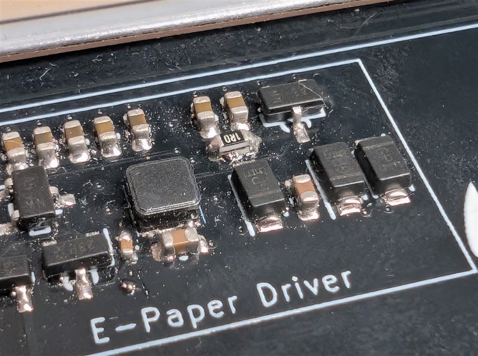
Because I don't plan to buy 0.47Ω resistors, I am going to change the schematic to use two 1Ω resistors in parallel.
This taught me an important lesson about PCB design: trace width and length seem irrelevant for most signals, but in edge cases, or when there are specific voltage or current requirements, they matter a lot.
6.6 Troubleshooting and challenges conclusion
All in all I learned a lot of new things while debugging my board and going through the ups and downs. I learned that a multimeter has important limitations that you need to know about. I learned that even small contamination from flux and solder paste can break sensitive chips and processes. And I learned how to handle complex SMD packages like the ESP32-S3 with many tightly packed pins, and also how important it is to calculate trace resistance rather than treating copper like a superconductor, which it is not.
7. Firmware
7.1 Toolchain and framework
As the framework I used the classic Arduino framework with the Arduino.h file inside VS Code with the PlatformIO extension installed, which handles the compiling, connecting to the board, library imports and much more.
I want to change to ESP-IDF for programming, which makes the whole code smaller, gives access to more advanced features and in general more control over the hardware. And I like to learn new things, so that sounds like a good idea for the future, especially when more hardware and a co-processor are on board.
7.2 Power management and sleep behaviour
The power management is not fully done yet, because I have not found enough time to write a firmware that uses 100% of the functionality the hardware could provide.
But there is a solid foundation for good power management and energy saving measures, because I can track exactly how many mA the whole board draws from the battery, and it can calculate the estimated time the battery will last. In addition to only measuring things, I can proactively save energy by completely turning off the 5V boost converter and all the connected LEDs. With 48 connected SK6805 LEDs dimmed to 0% and the boost converter idling it still takes around 150mA. Turning the whole rail off saves a lot of energy compared to just dimming the LEDs to 0%.
For the future even more power management hardware is planned, like dedicated current measurement for each section, so for the LEDs, the processor, the displays and so on, to get a better understanding of the power consumption and optimize it in the best way possible.
8. Where it stands now
8.1 What works
At this point all of the hardware works as intended. Every single functional block on the board has been used in the firmware, measured and used in a real application, and none of them is left out or bypassed with a wire. What is not finished is the firmware side of it, and that is what the next chapter is about.
The e-paper display renders text and images and can be updated over a web interface that the controller hosts itself. That means I can connect to the badge with a phone or laptop over WiFi, upload a new image or change the text, and the badge redraws itself without needing a cable or a reflash. Because it is an e-paper panel, the image stays on the screen afterwards even if the battery runs completely empty, which was one of the main reasons for choosing this display technology in the first place.
The controller also drives all 48 LEDs through the level shifter and can address every single one of them individually. Brightness and colour are freely controllable, and the LED rail can be switched off entirely when the LEDs are not needed, which matters a lot for runtime because the LEDs are by far the biggest consumer on the board.
On the power side everything comes up in the right order and all rails are properly initialised at boot. The 3.3V rail is stable and the 5V rail can be turned on and off at any time from the ESP via one GPIO. The charger works exactly as it should: when a USB-C cable is plugged in it charges the battery, when the cable is removed the system keeps running from the battery, and the switchover between the two happens without the rest of the system noticing anything at all.
The fuel gauge is alive and talking over I2C. It reports the battery voltage correctly and it reports the charge and discharge current correctly, both while the charger is running and while the badge is running on battery only. As described in chapter 6.4, it was in fact the fuel gauge that was right the whole time and my multimeter that was wrong, so at this point I trust it a lot more than I did at the beginning.
USB works for both flashing and serial output, so the whole development loop runs over a single cable without any external programmer.
8.2 What doesn't work yet
The one thing that is not finished is the state of charge estimation of the fuel gauge.
The raw values are fine. The gauge sees the correct voltage and it measures the correct current in both directions. What it does not get right yet is the derived information, so the remaining percentage and the estimated time until the battery is full or empty.
While discharging, the first 90% drop away in roughly the first 20% of the actual runtime, and after that the reading sits below 10% for a very long time while the badge just keeps running. Charging shows the same pattern in the other direction: it sits at some percentage and tells me one hour left, and one hour later it sits at around the same percentage and still tells me one hour left. Then at some point it climbs faster and reports full.
So the curve is compressed at one end and stretched at the other, which is a strong hint that the gauge is not working with a correct model of my battery, rather than that anything is broken. Right now I see two possible explanations and I have not ruled out either of them.
The first one is a configuration problem in my firmware. The gauge needs to know the design capacity of the cell and a few parameters describing where the cell is considered empty. If those values do not match the cell I actually use, every percentage it derives from them is going to be off in exactly this kind of way.
The second one is that the gauge simply has not learned the battery yet. This type of gauge builds its model over complete charge and discharge cycles, and I have not completed more than maybe one and a half full cycles so far. A 10000mAh battery takes a considerable amount of time to run empty, so getting through several full cycles is less a matter of debugging and more a matter of patience and monitoring.
Another thing that is not working the way I want it yet is the menu. There are three things that can be displayed on the e-paper display: name and icon, battery information, and WiFi information. Switching between these menus takes about 20s each, which is quite a long time just to see your battery usage. But this is not a bug in itself, it is a technical limitation of the e-ink display. In the future I will use an OLED screen for that kind of menu.
9. Next steps
9.1 My vision of the finished project
The badge already fulfills the basic tasks a badge needs to do: show a name and optionally look cool with a bunch of LEDs.
But for me that is not an end, it is a starting point. Everything below is stuff I want to add to make it cooler, but also more practical. Some of it is already planned in detail, some of it is still just an idea, and the order in which I get around to it will probably depend on how hard each part turns out to be.
9.1.1 Light sensor
When you walk into a building coming from outside, or the other way round, the LED brightness is basically always not optimal. You can change it with the brightness button, but every time the lighting around you changes, whether that is sunlight, room light or a dark hallway, you have to adapt it manually again.
I want to put a small ambient light sensor on the board so the badge can dim the LEDs automatically: brighter in direct sunlight so you can still see the colours, and much darker when you enter a dark room so it does not blind everyone around you. As a nice side effect this also saves a lot of energy, because the LEDs are the biggest consumer on the whole board and running them at full brightness indoors is simply wasted power.
9.1.2 NFC
Currently there is a small NFC sticker on the outside of the PCB where you can put a linktree or something similar. That works, but it is a sticker and it can only ever contain what I wrote onto it once.
What I actually want is this: two people wearing these badges hold them against each other and both of them directly exchange a digital business card, a linktree or whatever other information they want to share. That data could be shown directly on the screens or saved into a custom badge app that is connected over BLE.
But it should not only support badge to badge exchange. When you hold a normal smartphone against it, the badge should present itself as an ordinary NFC tag, so that anyone can read it without needing an app or a badge of their own.
I already selected a chip for this approach: the NXP PN7160.
9.1.3 Reverse charging
At conventions or fairs it happens all the time that you drain your phone and left your power bank back at the hotel. The badge has a 10000mAh battery inside, so it would be a waste not to let it charge your phone as an emergency power bank.
For this feature I need to decide whether I want to keep the charging chip I currently use and utilize the 5V boost converter to charge the phone, or whether I switch to a new charging controller which natively supports reverse charging. At this moment I tend to go with the second option.
9.1.4 USB Power Delivery
For faster charging I want to implement a USB Power Delivery controller which can draw more than 5V from power supplies that support this feature too. This results in greatly faster charging speeds.
9.1.5 OLED screens
The e-paper display is great for the name, because it stays readable without power and looks clean, but it takes about 20s for a single refresh. That makes it unusable for anything that changes often, and it is the reason why navigating the small settings menu is so uncomfortable right now.
Small OLED screens would solve exactly that: menus, battery and WiFi status, notifications, or anything else that updates more than once every couple of minutes. The e-paper keeps doing what it is designed for, and the OLEDs take over everything dynamic.
9.1.6 LoRa
LoRa opens up completely new possibilities, mainly keeping a link between two badges that paired over NFC before. They could send each other short messages, ping each other, or signal something without needing any WiFi, any mobile network or any infrastructure at all. At a convention where the WiFi is overloaded and the mobile network is dead because a few thousand people are standing in the same hall, that is a real advantage and not just a gimmick.
All badges would build up a mesh network, and this way, with enough people using it, it would easily cover giant areas.
This would be direct badge to badge LoRa, not LoRaWAN. LoRaWAN needs a gateway and a network server, which is exactly the infrastructure I want to be independent of.
9.1.7 Co-processor
For the LoRa functionality I am going to use an STM32 with built in LoRa. Adding a second processor has several reasons.
The first one is that I want to learn how to program an STM32 and how to handle the communication between a main processor and a co-processor, which is a pattern I have not worked with before.
But there are technical reasons as well: the STM32 is far more power efficient than the ESP32, so it can stay awake and listen for incoming messages while the ESP32 is in deep sleep. That opens up a whole new area of sleep modes and power saving, because the energy hungry ESP only has to wake up when there is actually something to do.
9.1.8 GNSS
With a GNSS module it becomes possible to track your friends and have the badge point you in their direction with the LEDs. That makes it super easy to find people on a crowded festival, or at conventions and fairs where they might be in a completely different building.
This obviously needs the LoRa link from above to work first, because the badges have to exchange their positions somehow. This feature won't be enabled by default, but only after explicitly linking two badges via NFC and enabling tracking.
9.1.9 UWB
UWB, short for ultra wideband, is the logical next step after GNSS. GNSS is often only accurate to around 10m and gets much worse or stops working entirely inside buildings, which is exactly where you need it at a convention.
UWB works the other way round: it does not tell you where you are on the planet, but it measures the distance and direction to another UWB device very precisely, in the range of a few centimeters, as long as you are within roughly 20m of each other. So GNSS gets you to the right building and the right corner of the hall, and UWB takes over for the last few meters and points you at the exact person.
9.2 Specific changes in rev 2.0
For the next revision 2.X I am implementing the light sensor and the OLED display. Maybe even two OLED displays, I am not sure about that yet.
These will not be ordinary OLED screens but transparent ones, which gives them a way fancier look and lets me overlap them with the e-ink display or with electrical components, so you can see the board through the screen while it is showing something.
Everything else from 9.1 is planned for later revisions, mostly because each of those blocks needs its own antenna work, and I would rather add them one at a time than debug four new radio sections at once.
