


"When I was young
I never needed fotoresist
And making circuit boards was just for fun
Those days are gone..."
Yes, it sounds like the beginning of an old famous song by Eric Carmen and that's what I'd like to talk about in this blog.
I'm Carlo Russo and I'm very interested in the theme of this project. I would like to go back in time and show you how I made my circuits when I was fifteen. I'm talking about the 1980s and the Internet did not provide inspiration and help to young makers.
My friends and I with a passion for electronics used to recycle old electronic components from radio or TV sets no longer working and to obtain electronic components and copper wire to make our FM transmitters, our "High fidelity" amplifiers or to make the crossover filters of our home-made loudspeakers.
Our source of inspiration were electronic magazines, the most famous in Italy in those years were "Nuova Elettronica" and "Elettronica Pratica" which proposed simple projects to be carried out with a couple of BJTs, some opamps or some SN74XX or CD4XXX integrated circuits.
I admit that for me the top was the legendary NE555. I've been playing with it for years making oscillators, multivibrators, timers, etc.
Even after many years, as an Electronics teacher, I have proposed it to my students many times on many occasions, astounding them for the incredible potential of such a simple and old device.
Making a printed circuit was a difficult thing.
I built the first circuits with connections made with copper wire but when the circuit was even slightly complex, this solution became impractical.
The magazines I bought published the image of the printed circuit in real size to give makers the opportunity to make it at home, but finding the photoresist and having the necessary equipment for photoengraving was out of my financial possibilities.
For a long time me and my friends have used an "artisanal method" to make printed circuits. We photocopied the image of the printed circuit and traced it on the vetronite board on the copper side using carbon paper. The trace that remained on the copper was then covered with nail polish and the board thus created was immersed in the solution of Ferric Perchloride, a chemical substance capable of dissolving the thin copper layer of the board in a few minutes and also capable of staining any item of clothing with even just a tiny droplet!
I remember we bought a bottle of this chemical and we used it for a very long time, sharing it among us.
Some years later, we found a way to make printed circuit boards by dissolving copper with a more homemade solution, even if it is just as smelly and dangerous for the skin and clothes.
Of course, thinking that today it is enough to send the file of our printed circuit to have in a few days cards produced with industrial quality, perhaps double-sided, etc.
In this blog I would like to retrace my origins and try to create a circuit like the ones I used to make in the very long and very hot Sicilian summer afternoons.
Phase 1: choice of project
We are talking about the 80s so I have no choice but to choose a circuit that represents those years.
Have you ever seen "Knight Rider", known in Italy as "Supercar" or "Galactica"? I was fascinated by the onboard scanner of David Hasselhoff's fantastic car and by the creepy Cylon viewer.


I will try to reconstruct a circuit that I made almost 40 years ago, with the means I had available at the time.
Obviously I will use a NE555 and a CD4017.

The first is an astable multivibrator, with a frequency
F = 7.3 Hz
The CD4017 acts as a divider by 10 and, after connecting the output pins two by two, except the first and the last, we will get the LEDs to turn on from right to left and from left to right continuously.
Phase 2: Realization of the printed circuit
Making a printed circuit without having a PC and software to automatically get the connections was very complicated.
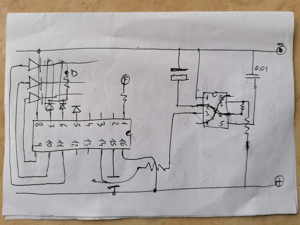
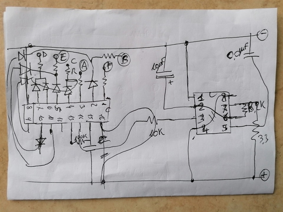
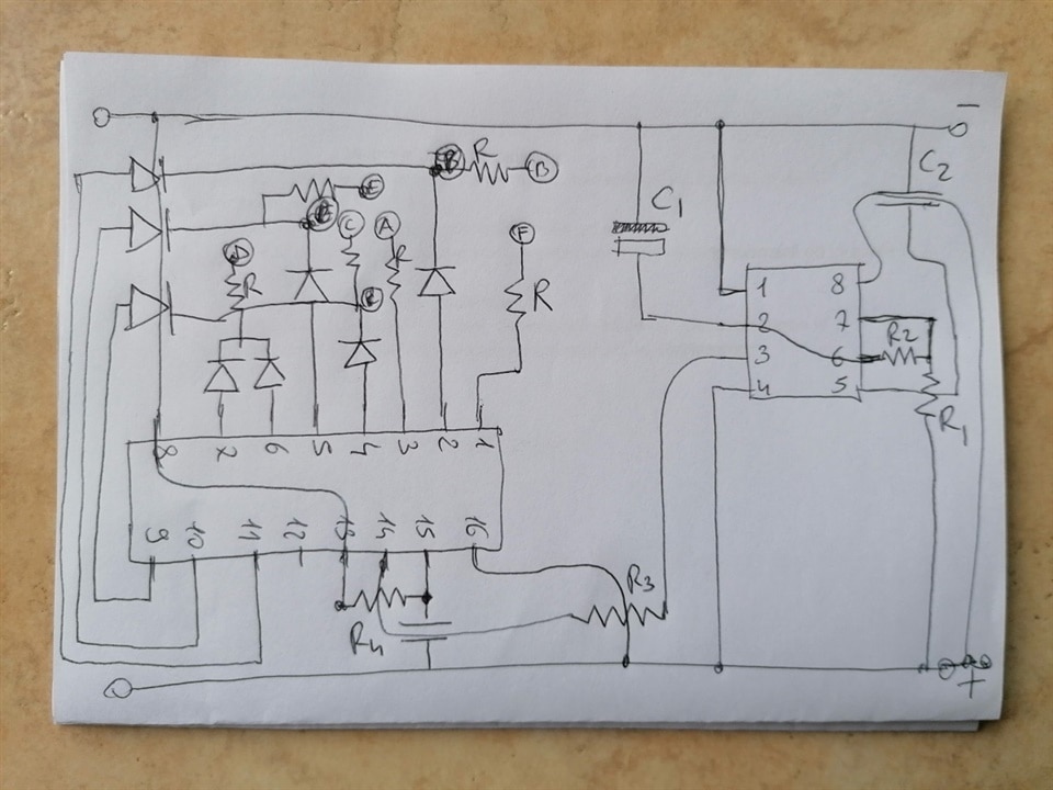
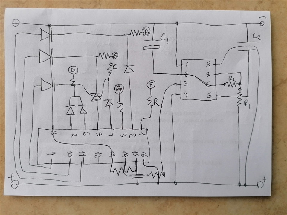
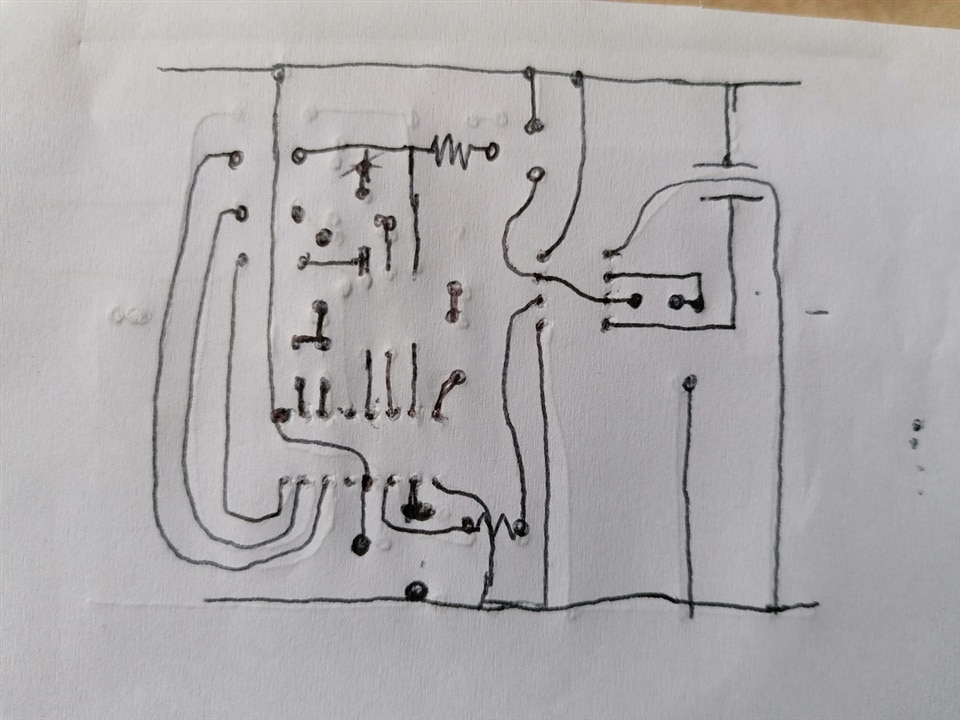
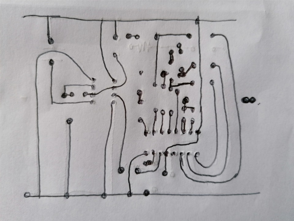
First I had to go from the wiring diagram to a physical assembly. At the beginning I used to take a piece of paper and a pencil and start drawing the electronic components starting from the more complicated ones, in this case the integrated circuits, positioning and rotating them on the sheet until you get easy connections.
In fact, it was unthinkable for me to work with copper-plated double-sided circuits so I had to prepare the components to have the least possible number of jumpers to make.
The photos represent the evolution of the "project" of the printed circuit, starting from the wiring diagram, to arrive at the traces that I will make on the copper plate.
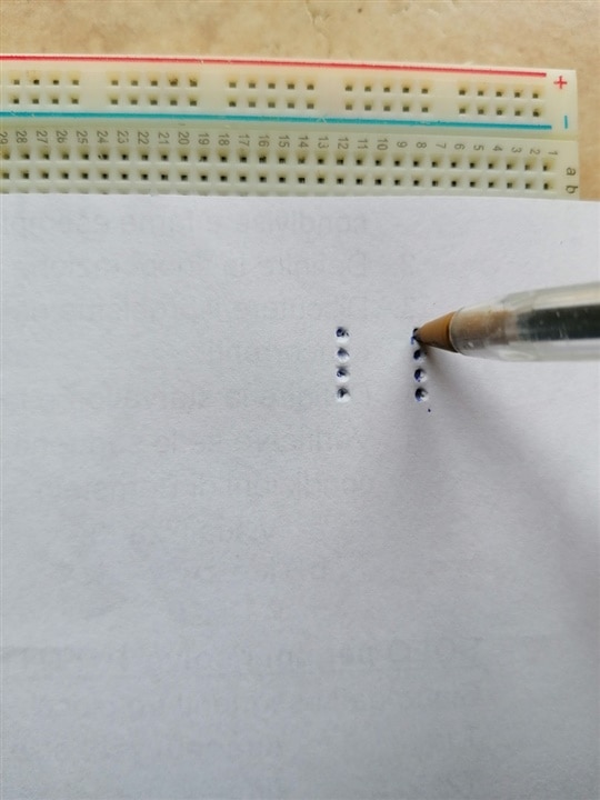
One of the most difficult phase is to correctly draw the IC's pins. I used to use a breadboard, I put a sheet of paper on it and use a pen to make holes where the IC's pin had to be placed.
| {gallery}From circuit to board |
|---|
|
|
|
|
|
|
|
|
This is what I have done so far. Unfortunately I started working on this revival project too late and in a busy school period that I cannot overlook. From here on I will tell what I did and the problems I encountered when making printed circuits many years ago.
and next...
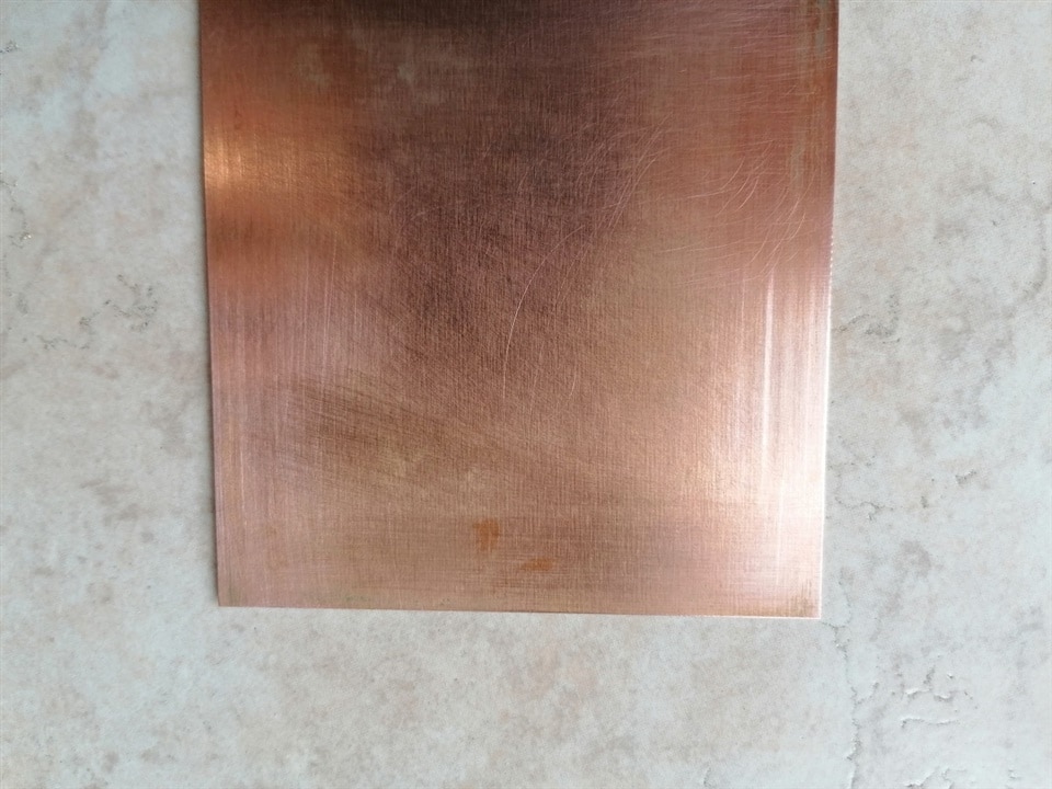
The next step is to trace the printed circuit design using a sheet of carbon paper to get the design of the connections on the copper.
At this point it is necessary to pass on the copper covering the traces left by the carbon paper with nail polish. The operation is long and complex, especially in correspondence with the pins of the printed circuits, the risk of creating short circuits is high.
After having covered all the connections with nail polish, the board is left to dry and after one hour the board can be immersed in the corrosive solution.
Then, the board has to be placed in a container filled with corrosive solution and floated with the copper-coated face down.
Periodically you have to move the board to facilitate the erosion of the copper and, after about an hour, the board will be perfectly made.
Once the acid has done its job and the board is ready, it must be washed to remove all traces of chemicals. This is a fundamental operation and must be done carefully since the boards that are not perfectly clean, after a few weeks, will become covered with a green oxide that will make them unusable.
After cleaning the card thoroughly, the nail polish used to protect the copper from the action of acid must be removed. For this purpose we will use a rag soaked in acetone and, after having removed all the enamel, we can move on to the drilling phase.
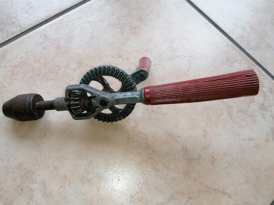
Also in this case, I will use the tool I was using then, a very old hand drill that belonged to my father, with which I will drill the holes necessary for the welding of the different components. Of course I'll start with the hardest parts to deal with, such as the pins on ICs. In the end, I will also make 4 slightly larger holes to be able to fix the board in the case.
Step 3: Welding the components
We are now ready for the soldering of the components on the board.
First we will solder the sockets of the two ICs and continue with the components from the smallest to the largest.
Step 4: Power up the circuit and cross your fingers!
Now everything is assembled and all that remains is to insert the two integrated circuits in their respective sockets and connect the power supply to the circuit.
This was the most terrifying phase for me.
I often plugged in my power supply and…. absolutely nothing happened. Every now and then the error was in some soldering and, with a good visual analysis of the circuit, I was able to get the circuit to work immediately. Sometimes the problem was more serious, a mistake in the circuit design and then it was necessary to act in a rather rude way, cutting the wrong tracks with a cutter and creating the new connections with external jumpers.
I almost always had the pleasure of seeing the circuit work, sooner or later!
Many years have passed since the last time I made a printed circuit at home and it was very pleasant for me to tell about it.
I hope not to have bored you and, as soon as I find a couple of afternoons all to myself I will show you the realization of my dream ...

Carlo

