


The Arduino MKR Vidor 4000 is a powerful but also mysterious board. The FPGA gives it a performance boost over other Arduinos but its functions are very badly documented. There are also very few code examples available on the internet.
Mini PCIe connector of the Vidor
I took a closer look at the Mini PCIe connector and wanted to see which functions are available at these pins.
This connector has 52 positions and the pinout can be grabbed from the official schematics of the board:
| Pin | Usage on Vidor | Usage on Mini PCIe card | Usage on Mini PCIe card | Usage on Vidor | Pin | |
|---|---|---|---|---|---|---|
| 1 | WM_PIO2/PEX_PIN1 | WAKE# | +3V3AUX | +3V3 | 2 | |
| 3 | WM_PIO3/PEX_PIN3 | COEX1 | GND | GND | 4 | |
| 5 | WM_PIO4/PEX_PIN5 | COEX2 | +1.5V | PEX_PIN6 | 6 | |
| 7 | WM_PIO34/PEX_PIN7 | CLKREQ# | UIM_PWR | PEX_PIN8 | 8 | |
| 9 | GND | GND | UIM_DATA | PEX_PIN10 | 10 | |
| 11 | PEX_PIN11 | REFCLK- | UIM_CLK | PEX_PIN12 | 12 | |
| 13 | PEX_PIN13 | REFCLK+ | UIM_RESET | PEX_PIN14 | 14 | |
| 15 | GND | GND | UIM_VPP | PEX_PIN16 | 16 | |
| 17 | WM_PIO24 | RESERVED | GND | GND | 18 | |
| 19 | WM_PIO25 | RESERVED | W_DISABLE# | PEX_PIN20 | 20 | |
| 21 | GND | GND | PERST# | PEX_RST | 22 | |
| 23 | PEX_PIN23 | PERn0 | +3.3VAUX | +3V3 | 24 | |
| 25 | PEX_PIN25 | PERp0 | GND | GND | 26 | |
| 27 | GND | GND | +1.5V | PEX_PIN28 | 28 | |
| 29 | GND | GND | SMB_CLK | PEX_PIN30 | 30 | |
| 31 | PEX_PIN31 | PETn0 | SMB_DATA | PEX_PIN32 | 32 | |
| 33 | PEX_PIN33 | PETp0 | GND | GND | 34 | |
| 35 | GND | GND | USB_D- | USB_DM | 36 | |
| 37 | GND | GND | USB_D+ | USB_DP | 38 | |
| 39 | +3V3 | +3.3VAUX | GND | GND | 40 | |
| 41 | +3V3 | +3.3VAUX | LED_WWAN# | PEX_PIN42 | 42 | |
| 43 | GND | GND | LED_WLAN# | PEX_PIN44 | 44 | |
| 45 | PEX_PIN45 | RESERVED | LED_WPAN# | PEX_PIN46 | 46 | |
| 47 | PEX_PIN47 | RESERVED | +1.5V | PEX_PIN48 | 48 | |
| 49 | PEX_PIN49 | RESERVED | GND | GND | 50 | |
| 51 | PEX_PIN51 | RESERVED | +3.3VAUX | +3V3 | 52 |
So the Vidor is somehow compatible to any standard Mini PCIe header used in computers. At least the GND and 3.3V pins are at the same location as well as the USB pins. On the Vidor the USB pins on the Mini PCIe connector are directly connected to the Micro USB connector on the other end of the board. So when plugged into a Mini PCIe socket on a computer it might be possible to programm the Vidor without using an additional USB cable.
After reset and when nothing is programmed all these pins are inputs. So nothing bad should happen if you plug it into your computer. But care must be taken when you programm the pins. Putting a high level (3.3V) on some of the 1.5V pins might carry some risk of damage.
Using the pins as GPIOs is quite simple. Actually it is already shown in the VidorTestSketch ( https://github.com/vidor-libraries/VidorPeripherals/blob/master/examples/VidorTestSketch/VidorTestSketch.ino ):
  // Ok, so we know now that the FPGA contains the extended GPIO IP
  // Please refer to the online documentation for the actual pin assignment
  // Let's configure pin A0 to be an output, controlled by the FPGA
  FPGA.pinMode(33, OUTPUT);
  FPGA.digitalWrite(33, HIGH);
The difficult part is to figure out why they use 33 as pin number. It is somehow common knowledge that MKR pins (AREF,A0..A6, D0..D14) have the numbers 32 to 54 assigned. So A0 is 33, A1 is 34 and so on. D14 is 54.
But what about the pins on the Mini PCIe connector? When you dig deep into the Arduino Vidor Forum you find a spreadsheet with the mapping:
https://docs.google.com/spreadsheets/d/1oAL1Iz39eCHi0IVyMiTRyekmzJg5TgeyO5t0fN6Vl4U/edit#gid=0
The tab "miniPCIe pinout" shows the mapping.
Mini PCIe connector pin | Name | Number in FPGA (software) | Comment |
|---|---|---|---|
| 22 | PEX_RST | 0 | |
| 6 | PEX_PIN6 | 1 | |
| 8 | PEX_PIN8 | 2 | |
| 10 | PEX_PIN10 | 3 | |
| 12 | PEX_PIN12 | 4 | |
| 14 | PEX_PIN14 | 5 | |
| 16 | PEX_PIN16 | 6 | |
| 20 | PEX_PIN20 | 7 | |
| 28 | PEX_PIN28 | 8 | |
| 30 | PEX_PIN30 | 9 | |
| 32 | PEX_PIN32 | 10 | |
| 42 | PEX_PIN42 | 11 | |
| 44 | PEX_PIN44 | 12 | |
| 45 | PEX_PIN45 | 13 | |
| 46 | PEX_PIN46 | 14 | |
| 47 | PEX_PIN47 | 15 | |
| 48 | PEX_PIN48 | 16 | |
| 49 | PEX_PIN49 | 17 | |
| 51 | PEX_PIN51 | 18 | |
| 11 | PEX_PIN11 | 19 | this pin is only an input |
| 13 | PEX_PIN13 | 20 | this pin is only an input |
| 23 | PEX_PIN23 | 21 | this pin is only an input |
| 25 | PEX_PIN25 | 22 | this pin is only an input |
| 31 | PEX_PIN31 | 23 | this pin is only an input |
| 33 | PEX_PIN33 | 24 | this pin is only an input |
And for my test this proved to be right.
VidorBreakout board
To access the pins one could directly solder cables to the pads which is a bit tricky or use an adapter. I couldn't find a good adapter so I made my own. You can find the data here:
https://github.com/generationmake/VidorBreakout

The breakoutboard connects all GND and 3.3V pins and brings only the GPIOs seperately to the pinheader. Additionally the Vidor can be directly srewed onto the adapter with a M2.5 screw and both form a solid unit.
The design was made using 3D models and FreeCAD so that there is no collision.
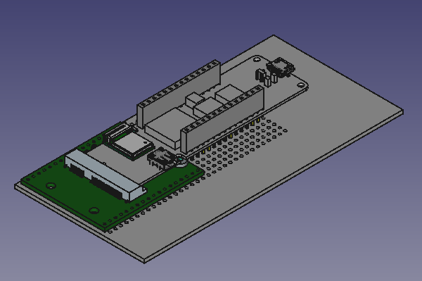
The adapte follows the 2.54 mm grid of the Vidor. So both could plugged into a breadboard. Althought you would need a special breadboard because the adapter is wider that a regular breadboard.

To demonstrate the function of the GPIOs and the adapter I made a LED sequence using 17 green 3mm LEDs with a 3.3 kOhm resistor connected to ground.

Unfortunately I couldn't find any more functions which are supported on the Mini PCIe connector pins. Hopefully this changes in the future.
Boards and parts are available at Aisler: https://aisler.net/p/VKRNBJOG
Software
This is the source code of my LED sequence:
#include "VidorPeripherals.h"
#define STARTDELAY 500

void setup() {
  Serial.begin(115200);
//  while (!Serial) {}
  // Let's start by initializing the FPGA
  if (!FPGA.begin()) {
    Serial.println("Initialization failed!");
    while (1) {}
  }

  // Let's discover which version we are running
  int version = FPGA.version();
  Serial.print("Vidor bitstream version: ");
  Serial.println(version, HEX);
  pinMode(LED_BUILTIN, OUTPUT);

  // Let's also ask which IPs are included in this bitstream
  FPGA.printConfig();

  // Ok, so we know now that the FPGA contains the extended GPIO IP
  // Please refer to the online documentation for the actual pin assignment
  // Let's configure pin A0 to be an output, controlled by the FPGA
  FPGA.pinMode(0, OUTPUT);
  FPGA.pinMode(1, OUTPUT);
  FPGA.pinMode(2, OUTPUT);
  FPGA.pinMode(3, OUTPUT);
  FPGA.pinMode(4, OUTPUT);
  FPGA.pinMode(5, OUTPUT);
  FPGA.pinMode(6, OUTPUT);
  FPGA.pinMode(7, OUTPUT);
  FPGA.pinMode(8, OUTPUT);
  FPGA.pinMode(9, OUTPUT);
  FPGA.pinMode(10, OUTPUT);
  FPGA.pinMode(11, OUTPUT);
  FPGA.pinMode(12, OUTPUT);
  FPGA.pinMode(13, OUTPUT);
  FPGA.pinMode(14, OUTPUT);
  FPGA.pinMode(15, OUTPUT);
  FPGA.pinMode(16, OUTPUT);
  FPGA.pinMode(17, OUTPUT);
  FPGA.pinMode(18, OUTPUT);
  FPGA.pinMode(33, OUTPUT);
  FPGA.digitalWrite(33, HIGH);

  // The same pin can be read by the SAMD processor
  pinMode(A0, INPUT);
  Serial.print("Pin A0 is ");
  Serial.println(digitalRead(A0) == LOW ? "LOW" : "HIGH");

  FPGA.digitalWrite(33, LOW);
  Serial.print("Pin A0 is ");
  Serial.println(digitalRead(A0) == LOW ? "LOW" : "HIGH");
}

void loop() {
  // put your main code here, to run repeatedly:
  int delaytime=STARTDELAY;

  FPGA.digitalWrite(1, HIGH);
  FPGA.digitalWrite(2, HIGH);
  FPGA.digitalWrite(3, HIGH);
  FPGA.digitalWrite(4, HIGH);
  FPGA.digitalWrite(5, HIGH);
  FPGA.digitalWrite(6, HIGH);
  FPGA.digitalWrite(7, HIGH);
  FPGA.digitalWrite(0, HIGH);
  FPGA.digitalWrite(8, HIGH);
  FPGA.digitalWrite(9, HIGH);
  FPGA.digitalWrite(10, HIGH);
  FPGA.digitalWrite(11, HIGH);
  FPGA.digitalWrite(12, HIGH);
  FPGA.digitalWrite(13, HIGH);
  FPGA.digitalWrite(14, HIGH);
  FPGA.digitalWrite(15, HIGH);
  FPGA.digitalWrite(16, HIGH);
  delay(delaytime);
  FPGA.digitalWrite(1, LOW);
  FPGA.digitalWrite(2, LOW);
  FPGA.digitalWrite(3, LOW);
  FPGA.digitalWrite(4, LOW);
  FPGA.digitalWrite(5, LOW);
  FPGA.digitalWrite(6, LOW);
  FPGA.digitalWrite(7, LOW);
  FPGA.digitalWrite(0, LOW);
  FPGA.digitalWrite(8, LOW);
  FPGA.digitalWrite(9, LOW);
  FPGA.digitalWrite(10, LOW);
  FPGA.digitalWrite(11, LOW);
  FPGA.digitalWrite(12, LOW);
  FPGA.digitalWrite(13, LOW);
  FPGA.digitalWrite(14, LOW);
  FPGA.digitalWrite(15, LOW);
  FPGA.digitalWrite(16, LOW);
  delay(delaytime);

  for(delaytime=STARTDELAY;delaytime-=100;delaytime>0)
  {
    digitalWrite(LED_BUILTIN, LOW);   // turn the LED on (HIGH is the voltage level)
    delay(delaytime);
    digitalWrite(LED_BUILTIN, HIGH);    // turn the LED off by making the voltage LOW
    FPGA.digitalWrite(1, HIGH);
    delay(delaytime);
    FPGA.digitalWrite(1, LOW);
    FPGA.digitalWrite(2, HIGH);
    delay(delaytime);
    FPGA.digitalWrite(2, LOW);
    FPGA.digitalWrite(3, HIGH);
    delay(delaytime);
    FPGA.digitalWrite(3, LOW);
    FPGA.digitalWrite(4, HIGH);
    delay(delaytime);
    FPGA.digitalWrite(4, LOW);
    FPGA.digitalWrite(5, HIGH);
    delay(delaytime);
    FPGA.digitalWrite(5, LOW);
    FPGA.digitalWrite(6, HIGH);
    delay(delaytime);
    FPGA.digitalWrite(6, LOW);
    FPGA.digitalWrite(7, HIGH);
    delay(delaytime);
    FPGA.digitalWrite(7, LOW);
    FPGA.digitalWrite(0, HIGH);
    delay(delaytime);
    FPGA.digitalWrite(0, LOW);
    FPGA.digitalWrite(8, HIGH);
    delay(delaytime);
    FPGA.digitalWrite(8, LOW);
    FPGA.digitalWrite(9, HIGH);
    delay(delaytime);
    FPGA.digitalWrite(9, LOW);
    FPGA.digitalWrite(10, HIGH);
    delay(delaytime);
    FPGA.digitalWrite(10, LOW);
    FPGA.digitalWrite(11, HIGH);
    delay(delaytime);
    FPGA.digitalWrite(11, LOW);
    FPGA.digitalWrite(12, HIGH);
    delay(delaytime);
    FPGA.digitalWrite(12, LOW);
    FPGA.digitalWrite(13, HIGH);
    delay(delaytime);
    FPGA.digitalWrite(13, LOW);
    FPGA.digitalWrite(14, HIGH);
    delay(delaytime);
    FPGA.digitalWrite(14, LOW);
    FPGA.digitalWrite(15, HIGH);
    delay(delaytime);
    FPGA.digitalWrite(15, LOW);
    FPGA.digitalWrite(16, HIGH);
    delay(delaytime);
    FPGA.digitalWrite(16, LOW);
  }
  for(delaytime=STARTDELAY;delaytime-=100;delaytime>0)
  {
    FPGA.digitalWrite(1, HIGH);
    delay(delaytime);
    FPGA.digitalWrite(2, HIGH);
    delay(delaytime);
    FPGA.digitalWrite(3, HIGH);
    delay(delaytime);
    FPGA.digitalWrite(4, HIGH);
    delay(delaytime);
    FPGA.digitalWrite(5, HIGH);
    delay(delaytime);
    FPGA.digitalWrite(6, HIGH);
    delay(delaytime);
    FPGA.digitalWrite(7, HIGH);
    delay(delaytime);
    FPGA.digitalWrite(0, HIGH);
    delay(delaytime);
    FPGA.digitalWrite(8, HIGH);
    delay(delaytime);
    FPGA.digitalWrite(9, HIGH);
    delay(delaytime);
    FPGA.digitalWrite(10, HIGH);
    delay(delaytime);
    FPGA.digitalWrite(11, HIGH);
    delay(delaytime);
    FPGA.digitalWrite(12, HIGH);
    delay(delaytime);
    FPGA.digitalWrite(13, HIGH);
    delay(delaytime);
    FPGA.digitalWrite(14, HIGH);
    delay(delaytime);
    FPGA.digitalWrite(15, HIGH);
    delay(delaytime);
    FPGA.digitalWrite(16, HIGH);
    delay(delaytime);
    FPGA.digitalWrite(1, LOW);
    delay(delaytime);
    FPGA.digitalWrite(2, LOW);
    delay(delaytime);
    FPGA.digitalWrite(3, LOW);
    delay(delaytime);
    FPGA.digitalWrite(4, LOW);
    delay(delaytime);
    FPGA.digitalWrite(5, LOW);
    delay(delaytime);
    FPGA.digitalWrite(6, LOW);
    delay(delaytime);
    FPGA.digitalWrite(7, LOW);
    delay(delaytime);
    FPGA.digitalWrite(0, LOW);
    delay(delaytime);
    FPGA.digitalWrite(8, LOW);
    delay(delaytime);
    FPGA.digitalWrite(9, LOW);
    delay(delaytime);
    FPGA.digitalWrite(10, LOW);
    delay(delaytime);
    FPGA.digitalWrite(11, LOW);
    delay(delaytime);
    FPGA.digitalWrite(12, LOW);
    delay(delaytime);
    FPGA.digitalWrite(13, LOW);
    delay(delaytime);
    FPGA.digitalWrite(14, LOW);
    delay(delaytime);
    FPGA.digitalWrite(15, LOW);
    delay(delaytime);
    FPGA.digitalWrite(16, LOW);
    delay(delaytime);
  }
  for(delaytime=STARTDELAY;delaytime-=100;delaytime>0)
  {
    digitalWrite(LED_BUILTIN, LOW);   // turn the LED on (HIGH is the voltage level)
    delay(delaytime);
    digitalWrite(LED_BUILTIN, HIGH);    // turn the LED off by making the voltage LOW
    FPGA.digitalWrite(16, HIGH);
    delay(delaytime);
    FPGA.digitalWrite(16, LOW);
    FPGA.digitalWrite(1, HIGH);
    delay(delaytime);
    FPGA.digitalWrite(1, LOW);
    FPGA.digitalWrite(15, HIGH);
    delay(delaytime);
    FPGA.digitalWrite(15, LOW);
    FPGA.digitalWrite(2, HIGH);
    delay(delaytime);
    FPGA.digitalWrite(2, LOW);
    FPGA.digitalWrite(14, HIGH);
    delay(delaytime);
    FPGA.digitalWrite(14, LOW);
    FPGA.digitalWrite(3, HIGH);
    delay(delaytime);
    FPGA.digitalWrite(3, LOW);
    FPGA.digitalWrite(13, HIGH);
    delay(delaytime);
    FPGA.digitalWrite(13, LOW);
    FPGA.digitalWrite(4, HIGH);
    delay(delaytime);
    FPGA.digitalWrite(4, LOW);
    FPGA.digitalWrite(12, HIGH);
    delay(delaytime);
    FPGA.digitalWrite(12, LOW);
    FPGA.digitalWrite(5, HIGH);
    delay(delaytime);
    FPGA.digitalWrite(5, LOW);
    FPGA.digitalWrite(11, HIGH);
    delay(delaytime);
    FPGA.digitalWrite(11, LOW);
    FPGA.digitalWrite(6, HIGH);
    delay(delaytime);
    FPGA.digitalWrite(6, LOW);
    FPGA.digitalWrite(10, HIGH);
    delay(delaytime);
    FPGA.digitalWrite(10, LOW);
    FPGA.digitalWrite(7, HIGH);
    delay(delaytime);
    FPGA.digitalWrite(7, LOW);
    FPGA.digitalWrite(9, HIGH);
    delay(delaytime);
    FPGA.digitalWrite(9, LOW);
    FPGA.digitalWrite(0, HIGH);
    delay(delaytime);
    FPGA.digitalWrite(0, LOW);
    FPGA.digitalWrite(8, HIGH);
    delay(delaytime);
    FPGA.digitalWrite(8, LOW);
  }
  for(delaytime=STARTDELAY;delaytime-=100;delaytime>0)
  {
    FPGA.digitalWrite(16, HIGH);
    delay(delaytime);
    FPGA.digitalWrite(1, HIGH);
    delay(delaytime);
    FPGA.digitalWrite(15, HIGH);
    delay(delaytime);
    FPGA.digitalWrite(2, HIGH);
    delay(delaytime);
    FPGA.digitalWrite(14, HIGH);
    delay(delaytime);
    FPGA.digitalWrite(3, HIGH);
    delay(delaytime);
    FPGA.digitalWrite(13, HIGH);
    delay(delaytime);
    FPGA.digitalWrite(4, HIGH);
    delay(delaytime);
    FPGA.digitalWrite(12, HIGH);
    delay(delaytime);
    FPGA.digitalWrite(5, HIGH);
    delay(delaytime);
    FPGA.digitalWrite(11, HIGH);
    delay(delaytime);
    FPGA.digitalWrite(6, HIGH);
    delay(delaytime);
    FPGA.digitalWrite(10, HIGH);
    delay(delaytime);
    FPGA.digitalWrite(7, HIGH);
    delay(delaytime);
    FPGA.digitalWrite(9, HIGH);
    delay(delaytime);
    FPGA.digitalWrite(0, HIGH);
    delay(delaytime);
    FPGA.digitalWrite(8, HIGH);
    delay(delaytime);
    FPGA.digitalWrite(8, LOW);
    delay(delaytime);
    FPGA.digitalWrite(0, LOW);
    delay(delaytime);
    FPGA.digitalWrite(9, LOW);
    delay(delaytime);
    FPGA.digitalWrite(7, LOW);
    delay(delaytime);
    FPGA.digitalWrite(10, LOW);
    delay(delaytime);
    FPGA.digitalWrite(6, LOW);
    delay(delaytime);
    FPGA.digitalWrite(11, LOW);
    delay(delaytime);
    FPGA.digitalWrite(5, LOW);
    delay(delaytime);
    FPGA.digitalWrite(12, LOW);
    delay(delaytime);
    FPGA.digitalWrite(4, LOW);
    delay(delaytime);
    FPGA.digitalWrite(13, LOW);
    delay(delaytime);
    FPGA.digitalWrite(3, LOW);
    delay(delaytime);
    FPGA.digitalWrite(14, LOW);
    delay(delaytime);
    FPGA.digitalWrite(2, LOW);
    delay(delaytime);
    FPGA.digitalWrite(15, LOW);
    delay(delaytime);
    FPGA.digitalWrite(1, LOW);
    delay(delaytime);
    FPGA.digitalWrite(16, LOW);
    delay(delaytime);
  }
}
Top Comments