Contents
Introduction
I’ve always been fascinated by radio technology, so this month’s Project14 sounded like an opportunity I wanted to try. This blog post describes a radio receiver board called the PlanetCatcher Model 1!
This project could be (I hope) interesting for anyone wishing to play with analog circuitry such as amplifiers, filters, transformers, audio and RF, but also digital control, software and perhaps digital signal processing as a follow-on project. All of these building-blocks are present on the board or discussed in this blog post. It is an easy-to-build project (no tiny parts) and cut-down versions of this project are also possible by selectively populating components, depending on what features are required.
There is a 4-minute video explaining the project here:
In terms of performance, with just a listening test, FM sounds acceptable – not super-hi-fi, but as good as a typical car stereo. In short wave (SW) mode, in a single evening, the board managed to pick up broadcasts from thousands of miles away with just a few meters of random wire as an antenna. There are lots of opportunities to improve the performance further.
The PlanetCatcher circuit board can connect to any microcontroller using a 3.3V I2C bus, and it outputs stereo audio, usable with headphones or ready for connection to an amplifier. This project is surface-mount, but all the parts are large and hand-solderable.
Eventually I’d like to build a wooden enclosure and fit a couple of speakers with amplifier and headphone socket for a fully-integrated home radio. Any microcontroller board, display and buttons or rotary encoders could be used to operate it.
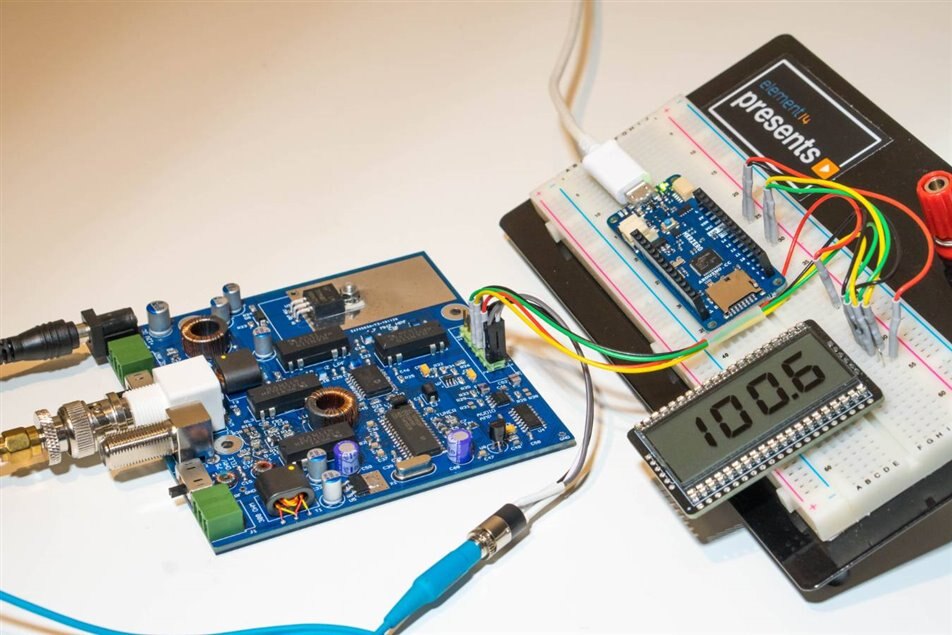
For now, to test the board, I temporarily connected an Arduino MKR ZERO board and wrote software that accepts keyboard inputs from a PC via the USB serial (UART) interface, to control all the board features. For the display I used an earlier LCD digit display project, but this could be replaced with other LED or LCD displays with some code modifications.
This blog post covers the design and how it was tested. The source code and schematics are attached, as are the PCB files for sending to a manufacturer, if anyone wishes to replicate this project.
Receiver Technology
Most radio receivers have a mix of analog and digital technology. Some of the older analog radio projects in books are no longer feasible due to components being obsolete. At one time it was common for radios to require many adjustable inductors and transformers, but those types of components have disappeared because modern radio architectures do not require them.
This project implements a ‘Low Intermediate Frequency (Low IF)’ architecture that gained popularity in the last couple of decades, but has now been succeeded by software defined radios (SDR) in many consumer products, although plenty of home and car radio designs being sold today still use Low IF. Many IoT radio modules use Low IF too So, this project isn’t using cutting edge SDR, but has a blend of analog and digital, and for learning purposes different parts of the design could be probed to explore how these receivers work.
This project may be using amongst the last of the highly-integrated radio chips that are easily hand-solderable (it is in a large SOIC-32 package). All modern radio chips are in much smaller packages, optimised for very high frequency communication or processing.
The particular chip used is obsolete, but still available from suppliers. Farnell had a decent amount of stock several weeks ago, but someone took them all : ( However, there are pin-compatible alternatives. NXP has around half a dozen pin-compatible chips in the range, with some feature differences; in particular, not all of them support the SW band. Other differences include the adjacent channel filtering method and low-FM band capability (used in some European countries). If the chip I used (TEF6606) is not obtainable, then TEF6601, TEF6607, TEF6614, TEF6616, TEF6617, TEF6621, TEF6623 or TEF6624 could be used (but check the datasheets to see if they support the features you want!). The chip that I used is still available from at least one distributor at the time of writing, as well as from ebay/aliexpress.
Design Overview
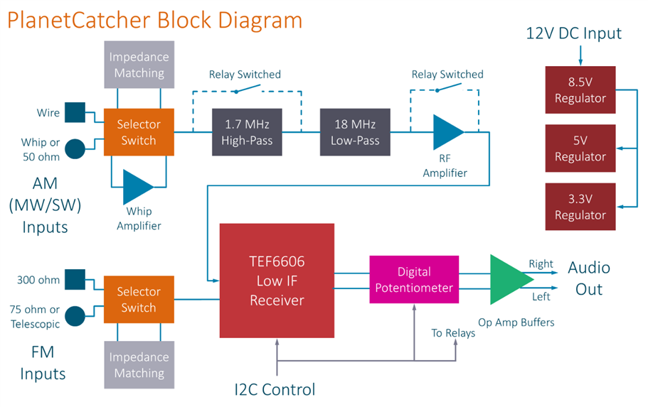
The diagram below shows what was implemented. Not all of these bits of functionality are needed. For example, if just an FM receiver was desired, then you could choose not to populate the parts related to the AM functionality.
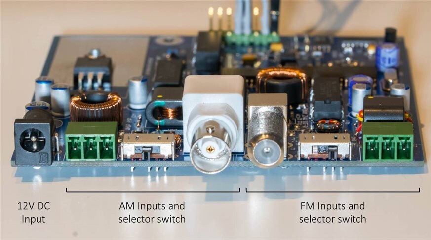
For flexibility, up to six different antenna types can be hooked up! There are 3-position selector switches for that. The switch position determines the impedance matching that is to occur to pass the received signal with reduced loss, and there is also a field effect transistor (FET) RF amplifier for whip antennas that have very high input impedance at the lower frequencies. The FM path is straightforward, but for the MW/SW path, there is an optional filter that can be switched under relay control. The intent is to filter out any high power MW broadcasts when it is desired to listen to weaker broadcasts. To help with that further, there is also another RF amplifier under relay control too.
Stereo analog signals are output from the TEF6606 chip. A digital potentiometer IC provides for volume control, and then the audio is buffered using op-amps, for driving an off-board amplifier (low-power headphones can be connected directly).
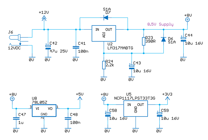
The board is powered from a 12V source. The main 8.5V regulator (the voltage is labelled 8V in the schematic in places, but it is actually 8.5V) powers the TEF6606 chip. The voltage is further dropped down to 5V for the digital potentiometer, and a 3.3V regulator is used too, for the digital logic. An I2C expander chip is used to control the 12V relays on the board.
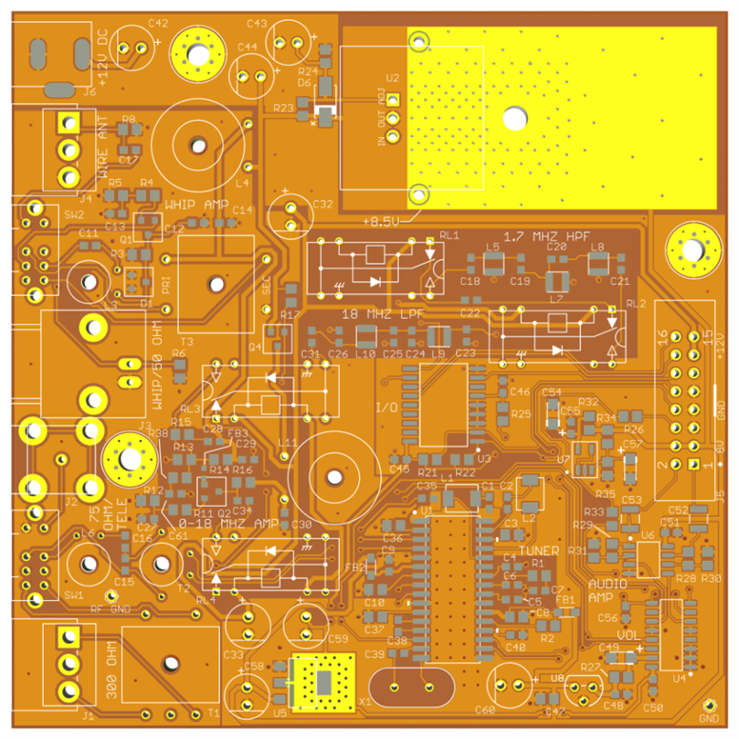
PCB Layout
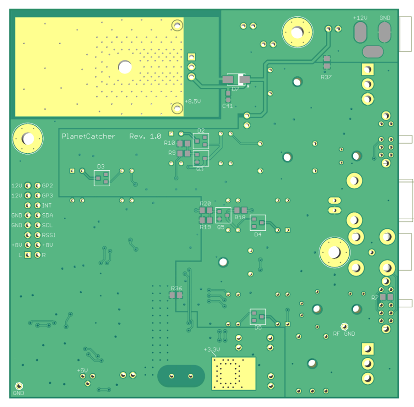
The PCB is a 2-layer board, 100x100mm sized, so it costs very little to get manufactured.
AM RF Path
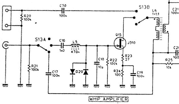
For the AM (MW and SW) inputs, I copied an existing whip antenna design from an old ‘AOR’ receiver service manual I found online, with very few changes - just a slightly simpler transformer output, and a replacement for the obsolete J310 JFET.
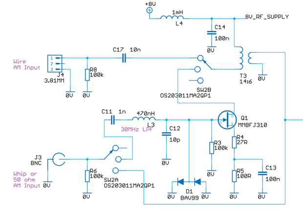
As can be seen, the AOR design has a nice implementation where three inputs can be selected using a dual pole 3-way selector switch. When the whip antenna input is selected, a FET amplifier is automatically enabled. At the output the AOR design has a transformer which will be unobtainable today, so a custom toroidal transformer is used for the PlanetCatcher. It is easy to hand-wind and the instructions are further below (several components need to be hand-wound for the PlanetCatcher). The implemented whip amplifier circuit is shown below. The dual pole switch was used such that the amplifier is only powered up when the signal needs to pass through it. The output transformer is used to lower the output impedance for the next stage. Some experimentation would be needed to design the transformer. Since I was going straight-to-PCB for the first prototype, I had to take a guess, and I think it’s reasonable because AM performance seems acceptable.
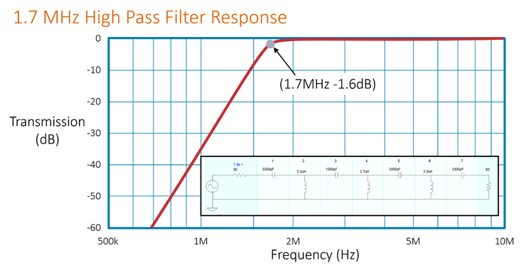
A free copy of ‘Elsie’ software was used to calculate the required inductors and capacitors for the filter stages.
Elsie is really easy to use; it is possible to specify a design topology and requirements, and the software will automatically design the filter and display a plot of the expected results.
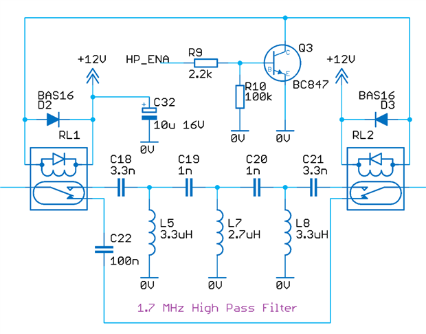
The schematic below shows the implemented design. A couple of relays are used at the input and output, in order to be able to bypass the filter by default. The filter is introduced into the signal path when the relays are energised.
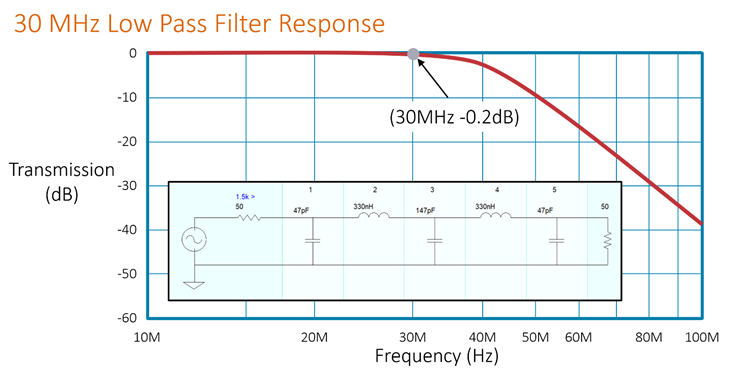
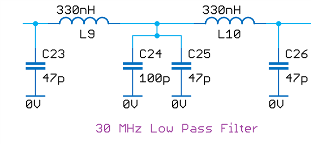
After the high-pass filter, the next stage is the low-pass filter shown below. The low-pass filter is intended for blocking anything beyond the short wave band. I’d initially speculated that the TEF6606 may allow tuning up to 30 MHz, so I’d designed the filter for that. However, the highest short wave frequency that the chip allows is 18 MHz. Ideally the filter needs to be redesigned for 18 MHz but I went ahead and used the 30 MHz design for now. If you re-compute the filter for 18 MHz, please do share the details.
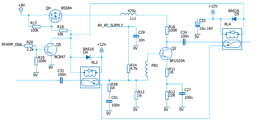
A single transistor amplifier stage follows the filters. A MOSFET and a couple of relays are used to power up the amplifier and switch the stage in or out. The transistor datasheet was examined to determine a suitable collector current, and that dictated the collector resistance and the base biasing resistors and total emitter resistance. Once I had ballpark values the design could be simulated but in reality I had to wait to see if the circuit could perform, since the simulation isn’t accurate without using specialist software.
The end result was that the amplifier did work, providing several dB of improvement in the demodulated audio quality (see further below in this blog post for details) but with experimentation it could be improved further. With hindsight I should have used a transformer on the output, because the input impedance of the chip is very low. I didn’t have a full chip datasheet to work with (lots of Internet browsing finally revealed a draft datasheet which was good enough to work from).
Finally, the output of the AM RF path is fed into the TEF6606 chip (see further below for the schematic for that).
FM RF Path
The path for the FM radio signal is simpler.
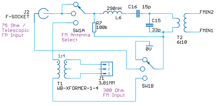
According to the TEF6606 draft datasheet, the FM section has an input impedance that looks like 300 ohm in parallel with 4 pF capacitance, at the center of the FM broadcast band. In other words, the impedance looks like 300 ohm in parallel with 410 ohm, i.e. 173 ohm at that frequency (no math is required; you can use online reactance calculators and parallel resistance calculators for all of this).
The desired impedance is either 300 ohm for FM folded dipole antennas (the sort that look like a large T-shape made of flattened tape), or a far lower value of the order of 37 ohm for a FM whip antenna, or around 75 ohm for a typical roof-top FM antennas. I decided to implement a 75 ohm input and a 300 ohm input, and any whip or single wire antenna can be still connected to the 75 ohm input for reasonable reception for portable use too.
If we want to have a 75 ohm input matched to the 173 ohm impedance, then one way is to use a small transformer. The turns ratio would need to be about 3:5 to achieve this (see https://www.changpuak.ch/electronics/broadband_transformer_matching.php to calculate this) and this approximately agrees with what the datasheet specifies in the application circuit. The particular transformer is unobtanium, so something custom is needed. Again, it was decided to hand-wind this and the instructions on how to do it are further below.
The components L6 and C6 form a resonant circuit at the lower end of the FM band, and C15 and the transformer primary form a resonant circuit at the higher end of the band. I copied those components from the TEF6606 datasheet.
For the matching of the 300 ohm antenna input, a single component can be used; a transformer that transforms the impedance by the ratio 4:1. It is described further below.
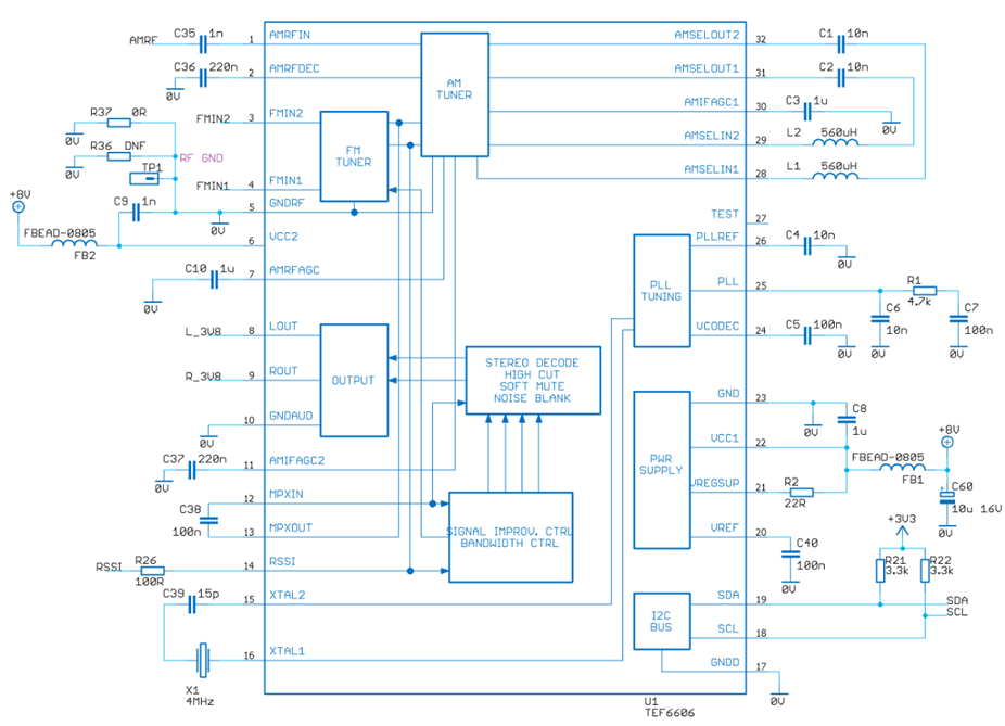
TEF6606 Schematic
The FM and AM paths end up at the TEF6606 receiver IC, at pins 4 and 1 respectively. There’s a lot going on inside the chip. I briefly explored the RSSI output on pin 14, and it could be connected to an ADC pin (after a voltage divider, to limit the range) on the microcontroller if desired; it is brought out to a pin on the main connector on the board.
The audio output appears on pins 8 and 9.
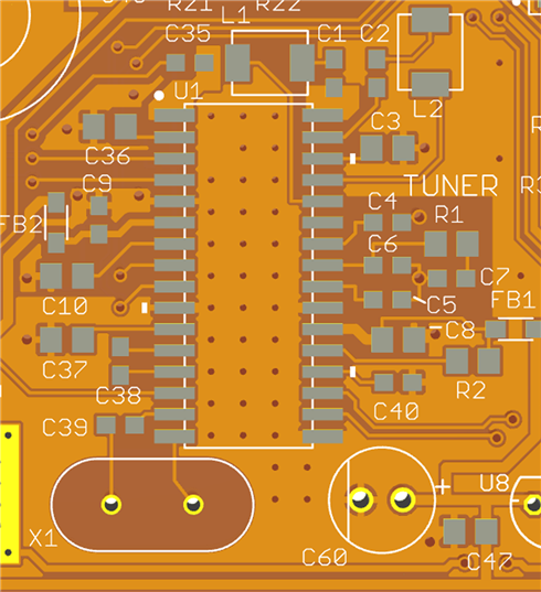
In terms of layout, according to a Chinese website (there really isn’t a lot of information on the chip, so Google translation came to the rescue) the chip can get warm, so the corner pins are used to dissipate some heat into the PCB. The center of the chip needs to be kept clear of traces other than ground, to avoid noise pick-up into the RF circuitry.
Volume Control
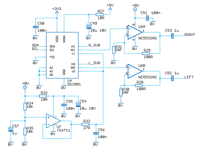
The output from the TEF6606 goes into a dual digital potentiometer circuit. The U7 component is used to generate a mid-level voltage so that any volume switching occurs as close as possible to that point, to reduce click sounds. The audio output is buffered, ready for an audio power amp (or headphones can be directly attached).
Off-Board Interface and Digital I/O
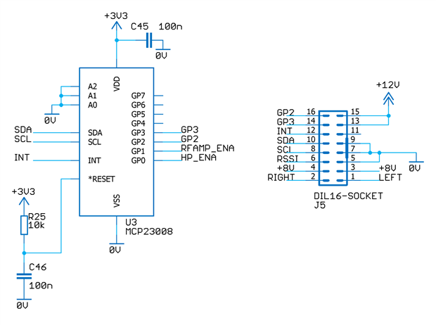
A 16-pin 0.1” connector/ribbon cable can be used to attach the PlanetCatcher to a microcontroller and to any external audio amplifier. The digital electronics is controlled using an I2C bus. An I2C expander is used to control the relays, and a couple of the I/O pins are brought out to the connector too. The pins could be used to control LEDs or to power up an audio amplifier.
Power Supplies
The PlanetCatcher board is powered from a single 12V DC supply. Linear regulators are used to reduce it to 8.5V (although it is marked +8V on the schematic, it is actually 8.5V), and to 5V and 3.3V. The relays on the board are operated from the 12V supply. The TEF6606 chip and the audio op-amps use 8.5V, and the volume control operates from 5V. The 3.3V supply is used for the digital circuits.
There is some space on the PCB used as a heatsink for the 8.5V regulator (the LM317 chip gets a little warm).
Building the Wound Components
There are seven wound components; four inductors and three transformers. All of these can be constructed using approximately 0.2mm (32 AWG or 35 or 36 SWG) diameter enamelled copper wire apart from transformer T1, which uses 30 SWG (28 AWG) kynar insulated wire (or perhaps CAT5 network cable wires could be used if they fit).
Inductors
The two smaller inductors use a T20-17 iron powder toroid, and the two larger inductors use a FT-50-43 or FT-50A-43 or Fair-Rite 5943000301 ferrite toroid. A ballpark calculation was done to determine the number of turns, and then it was verified with an LCR meter (which won’t be accurate due to the different measurement frequency, however these inductors are not being used in a role that requires precision.
L3: A T20-17 iron powder toroid is used, and 19 turns are wound around it.
L6: A T20-17 iron powder toroid is used, and 15 turns are wound around it.
L4: A FT-50-43 or FT-50A-43 ferrite toroid is used, with 48 turns (it doesn’t matter if the turns count is not precise)
L11: A FT-50-43 or FT-5A-43 ferrite toroid is used, with 33 turns (it doesn’t matter if the turns count is not precise)
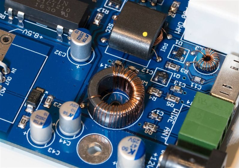
The photo below shows close-ups of two of the inductors; L3 and L4 are visible in this photo.
The ends of the enamelled copper wire were stripped of their enamel by heating the ends with an iron with a hot blob of solder on the tip. After a few seconds the enamel just burns away.
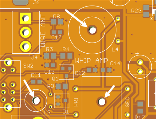
The toroids need securing; I’ve not glued them down yet, in case I make any tweaks to the design. The PCB has holes directly underneath where the toroids are to be placed; this could be useful for 3D-printed clips to be fashioned to hold the toroids in place perhaps.
Transformers
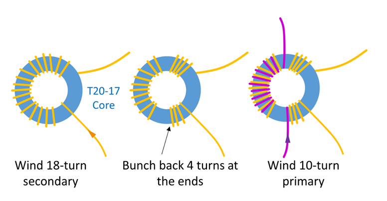
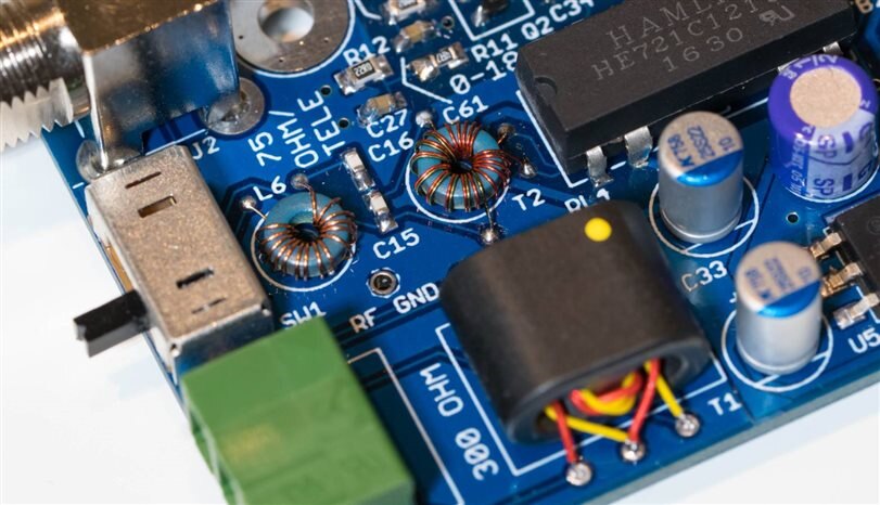
Transformer T2 is built with a T20-17 iron powder core and has an 18-turn secondary, and a 10-turn primary. I interspersed the winding as shown below.
Although ordinary enamelled copper wire can be used, if you can find ‘bifilar’ wire, it makes it easier to wind. There doesn’t seem to be any convenient source of such wire; I got lucky a while ago and found a seller on ebay to purchase a reel from. The photo below shows the resultant transformer using such wire.
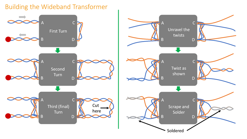
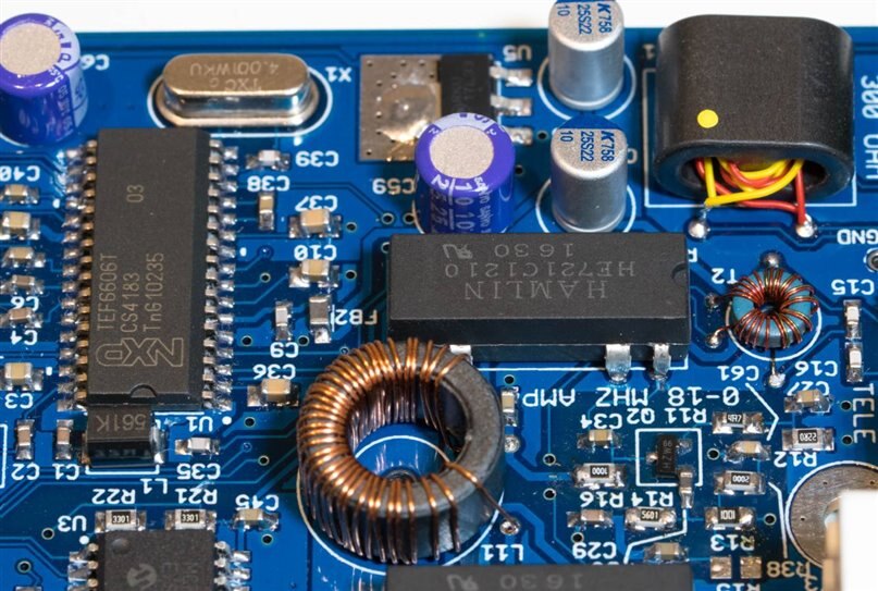
Transformer T1 (also visible in the photo above) is built with a Fair-Rite 28430003022843000302 binocular core (so-called for obvious physical reasons : ). It requires two lengths of wire to be twisted together. The aim is to create a transmission line for 150 ohm; I believe that can be achieved close to that value with the insulation on kynar wire, lightly twisted together. If it fits, then Cat 5 patch wiring could be used too (I didn’t check to see if it does fit), slightly looser twisted that it would normally be twisted. If you can find it and it fits, then PTFE insulated wire with slightly thicker insulation that Kynar wire would be better, because then it could be twisted slightly more. It is all insulation-material-dependent basically, since it is acting as the dielectric for the capacitance between the two wires.
Next, it needs to be assembled as shown in the diagram below. The red blob is just to indicate one wire end in an attempt for some clarity in the diagram.
The reason for the twists and the configuration is that this transformer comprises of two 150-ohm transmission lines after step 3 in the diagram has been completed (i.e. after the wire has been cut as indicated in that step). The sixth step ends up connecting the two transmission lines in parallel on the left side, and in series on the right side. This makes the impedance appear to be 75 ohm (half of 150 ohm) on the left side, and 300 ohm (twice 150 ohm) on the right side, across a wide range of frequencies (it needs to operate from about 60 MHz to 108 MHz, to cover the commonly-encountered FM bands). This design of transformer is known as a Guanella transformer after the person who invented this topology.
The photo below shows the view of the transformer from the other side. The yellow dot on the transformer marks location ‘A’ in the diagram.
Transformer T3 is simpler. It is visible in the photo below. It too is built using the same binocular core as T1. Enamelled copper wire (0.2mm) is used, and the primary winding has 14 turns, and the secondary side has 6 turns.
Using the Software
Currently the PlanetCatcher board is operated using an Arduino MKR ZERO board. The only pins that need connecting are SDA and SCL (for the I2C bus) and GND. Optionally an LCD display can be attached to the same I2C bus.
The code relies on the MKR ZERO USB UART being used to operate the radio. Any serial terminal can be used, at 115200 baud. The controls are shown in the table here. Eventually I’d like to have a proper control board with buttons, but that’s a project for another day.
| Keypress | Description |
|---|---|
| + | Increase frequency |
| - | Decrease frequency |
| q | Volume up |
| a | Volume down |
| s | Stereo on |
| m | Mono on |
| 1 | AM band (Broadcast band) |
| 2 | SW mode |
| 3 | FM mode |
| g | RF Amplifier on |
| b | RF Amplifier off |
| h | High Pass Filter on |
| n | High Pass Filter off |
Sensitivity Measurements
Receiver sensitivity is an end-to-end measurement; the thing being measured isn’t anything to do with RF at all – it’s an audio measurement : ) The general idea is to feed a weak known signal (usually a 1kHz modulated RF signal) at a known power level, into the antenna input, and then check the quality of the recovered audio output.
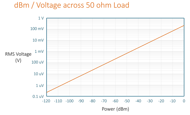
Power levels are measured in dBm, where the ‘m’ represents milliwatts. A sinewave of amplitude 220 mV RMS, across a 50 ohm resistor, will result in 1 mW of power being dumped in the resistor, and it is equal to 0 dBm. That’s at the top-right of the chart below. As suggested from the chart range, commonly encountered power levels could be far lower.
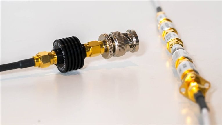
A signal generator might not generate such small signals, so one option is to generate a higher power output, and then put an attenuator or two (or a lot!) on the end.
The most popular method for speech (and for AM broadcast and SW bands this is relevant too) is called SINAD which is short for SIgnal to Noise And Distortion. The SINAD measurement results in a value in dB. The higher the value the better the audio quality. Often a value is chosen (e.g. 10dB) and then the signal level to the receiver is adjusted until that chosen value is achieved. Thus, the actual result is written as (say) Sensitivity: -110 dBm for 10 dB SINAD. Usually the test frequency is also supplied, e.g.: Sensitivity at 1 MHz: -110 dBm for 10 dB SINAD.
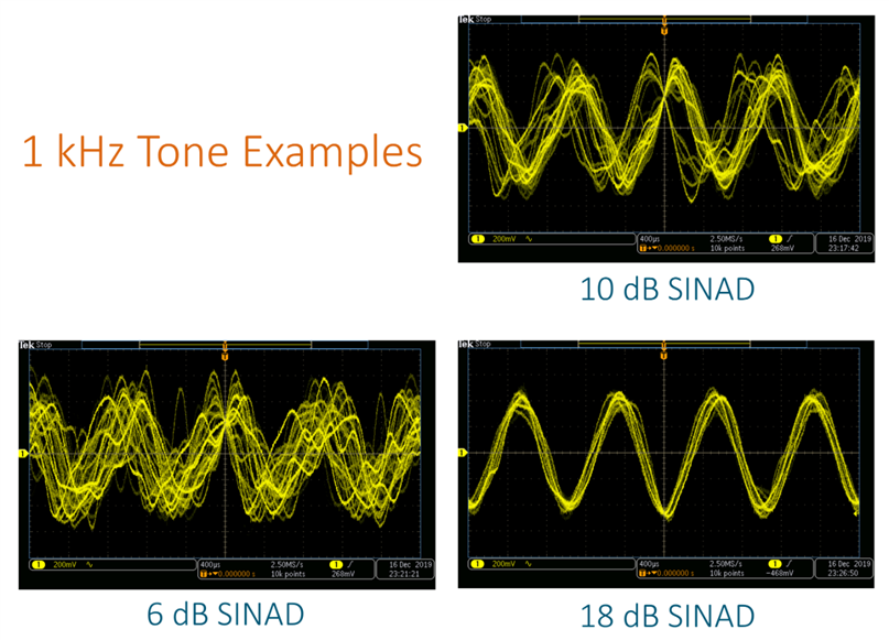
It’s generally considered that 6dBm SINAD is a limit of intelligibility, and that 10dB SINAD will be fairly usable to understand a conversation.
Incidentally, the 6dB level is fairly easy to judge just by listening to the signal. Once you’re getting close to the point where you can only just detect the received signal over the noise, then that’s around 6dB SINAD.
In the past, dedicated instruments would be used to perform this measurement, but an alternative approach is to use a PC. The procedure was to generate an AM signal with 1kHz audio tone at a known power level, and then pass it through lots of attenuators to drop the level to below -100dBm. The audible tone from the receiver audio output was captured using a PC sound card and passed into MATLAB. MATLAB has a sinad function to compute the result in seconds. With a bit of code, you can get MATLAB to output SINAD values each second, so you can adjust things while watching the PC measurement.
I repeated this test at different power levels until I reached 10dB SINAD. The power level at that point was -114 dBm for the 50 ohm input, at 997 kHz. This is quite good, definitely adequate for a home receiver. At a few different SW frequencies that I tested, I required signal levels of -111dBm to -115dBm to achieve 10dB SINAD.
The MATLAB code required to function as a SINAD measurement tool is shown below.
while 1>0
    recobj=audiorecorder(44100, 16, 1, 1);
    record(recobj);
    pause(2);
    stop(recobj);
    y=getaudiodata(recobj);
    r=sinad(y, 44100)
end
The fourth parameter to the audiorecorder function is an identifier to the sound card. To get that identifier, type:
info=audiodevinfo
info.input.name
info.input.ID
This ten-second video recording contains an example 1 kHz tone being received at 10 dB SINAD, and shows what commands to type in MATLAB to calculate that, using a .wav file as a source.
Signal Processing with MATLAB
The radio might benefit from analog speech processing, or digital signal processing (DSP) for the AM bands. In the past, a radio may have filters for the speech band, and even notch filters for getting rid of whistles or unwanted tones. However, out of curiosity I explored what some of the digital algorithms could do, using MATLAB. To do that I recorded the output from the receiver, and then uploaded it into MATLAB and ran some code in a library called VOICEBOX.
It was quite interesting, it did seem to kill off a lot of the noise from the short wave recordings, although occasionally the output sounded slightly robotic.
Here are the MATLAB commands to do the processing:
[y,fs,wmode,fidx]=v_readwav('c:\c_root\music\source.wav');
e(:,1)=v_ssubmmse(y(:,1), fs);
e(:,2)=v_ssubmmse(y(:,1), fs);
f=v_writewav(e, fs, 'c:\c_root\music\processed-output.wav', '*', 0, 3, []);
The source and processed output can be listened to in the recording here:
Summary
This project grew larger than expected! Anyway, with a bit of effort, it proved possible to build a receiver board that could be used for future enhancements and experimentation. There is lots of scope for improvement. It would be nice to develop some sort of audio processing board for it!
The board files, schematics, parts list and source code are attached to the blog post.
Thanks for reading.



Top Comments
-

fmilburn
-
Cancel
-
Vote Up
+4
Vote Down
-
-
Sign in to reply
-
More
-
Cancel
-

shabaz
in reply to fmilburn
-
Cancel
-
Vote Up
+5
Vote Down
-
-
Sign in to reply
-
More
-
Cancel
-

fmilburn
in reply to shabaz
-
Cancel
-
Vote Up
+4
Vote Down
-
-
Sign in to reply
-
More
-
Cancel
Comment-

fmilburn
in reply to shabaz
-
Cancel
-
Vote Up
+4
Vote Down
-
-
Sign in to reply
-
More
-
Cancel
Children