A bit of history
Ever since my dad made me discover the wonderful world of electronics back in the 1980s, we never had a proper Lab supply but always used a model railroad transformer, battery packs or more recently USB power bricks.
As I was moving quite a lot for my studies and work, my “electronics” lab had to be quite lightweight, which means that things like an oscilloscope, proper lab PSU or even soldering station were not even on the “buy list”.
Fast forward to 2009 when settling down was very much in its final stages which made getting a proper electronics setup come back at the top of the priority list. I could have bought most things “ready-made” at the shop but this was quite pricey. As a computer engineer by trade, I had a few AT/ATX power supplies lying around and thought: hey, why wouldn’t I save some money and simply use one with a panel in front. This has the advantage of providing 5 different voltages, a thing that a regular lab supply cannot do for any reasonable price.
But in the true “Shadok” spirit that I’m still fighting against nowadays, I went full on with the “why make things simple when they can be complicated?” motto and decided that I wanted a protection circuit with over current protection shutting down the output until a manual reset occurs.
I don’t exactly remember how I ended up selecting the MAX4373 but looking at its datasheet, my “cost cutter” mind thought that I could measure the series resistor of a MOSFET and thus save on components count as over current signaled by the comparator would then simply turn off the N Channel MOSFET. But what came up quite rapidly was that this is an almost impossible task, especially because of the requirement to drive the N channel MOSFET from the high side, which brought the LTC1693 chip into the picture.
And because coming by precision shunt resistors for large loads was very expensive, there are two MOSFETs in parallel, both in series with the load, so that a small part of the current is going through a relatively large resistor used as the sensing element for MAX4373.
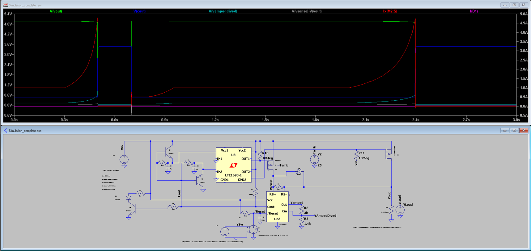
As this was quite a step up from the circuits I had created before, I decided to simulate them and LTSpice was at the time the only viable option for a hobbyist not capable of forking hundreds of dollars just for software.
For reference here are the LTSpice results for the 5V over current protection:
This was discussed in NNTP newsgroups but this is also about that time that I heard of Element14 and that I registered to start asking questions about my little project. Sadly, but not surprisingly, there are no traces of this anywhere to be found easily.
The discussion led to a partial redesign where I would use an ATX supply instead of AT which was already old even in 2010. This meant losing the built-in -5V but that’s something that I solved by placing a 79L05 on the -12V line with just stricter current limits on it.
And for good measure, I also added a voltage reference with a LT1460 chip alongside a variable voltage/current source based on the “Lab supply” typical application described in the LT3080 datasheet.
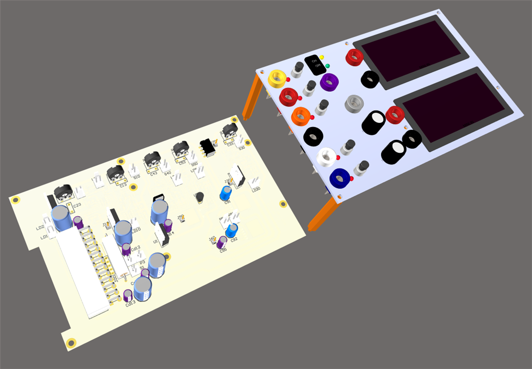
With all this settled, I decided to design my own PCB for it, along with full 3D models so that I could “view” the result before I ordered parts for it. This was because of being burnt before on other projects where components would collide with buttons or were not getting out of the case the way I wanted things to work, which lead me to the following 3D render of the setup:
And finally, I placed orders on various websites to get all the required parts and figured I could get it made into the real thing during the month of paid time off I would get in December 2010 following the birth of my first child.
Ah the naiveness that I had at the time!
Of course, the baby took all the time and energy we both had and this project, like many others, got put on hold for an indefinite amount of time. Fast forward fifteen years and that project is still on hold, with all those components/cables/copper board waiting for better times in a plastic bag that has started to degrade into bits and pieces.
To be honest, it never came back close to the top of my projects list because in the meantime I had purchased a lab supply of decent quality for a very reasonable price which has been much easier to come by in the past five years or so.
But the Spring clean project is the nudge I had been needing and even if it won’t be as useful as fifteen years ago, I decided to bring it back to life.
Preparing the revival
To begin this revival, I had to restart the development virtual machine that I used at the time, fire up the design software inherited from my student years and see if they would still run properly after all this time. Luckily, they did and so was able to create a BOM for the project. With that I could just verify what was still there and what parts had been used for other projects during those years:
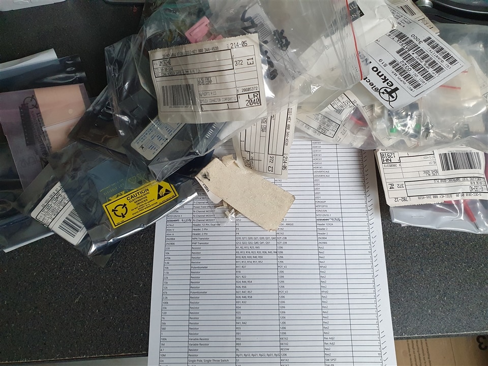
To my great surprise, only four references were missing! But I also discovered that I failed basic math in 2010 as I ordered 20 crimp contacts for the 20 2-pin connectors that I need…
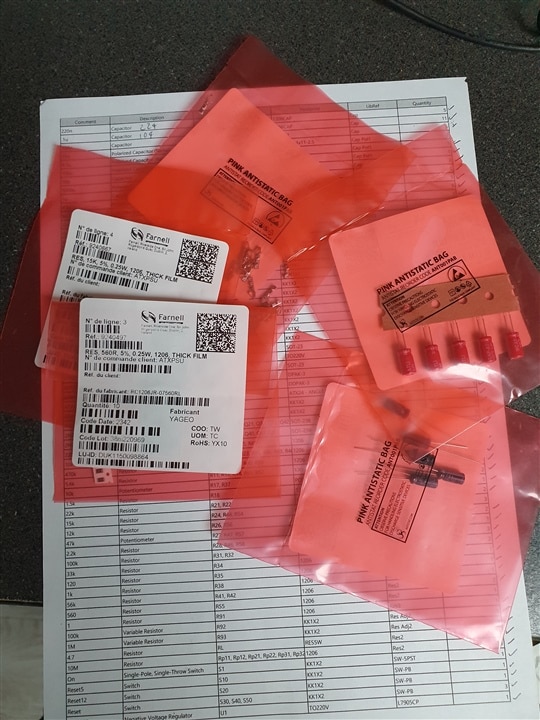
One order on the Farnell website later, I was able to check every item on that list:
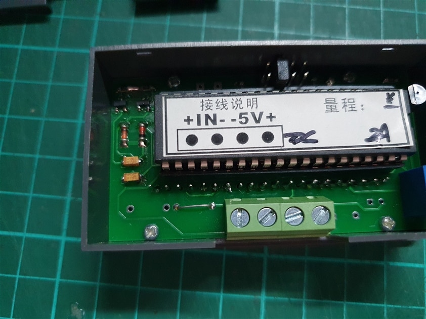
Next step was to identify the wiring of the two “meter” modules. As you can see on the pictures below, there are no markings on the outside of the housing to indicate pin assignments:
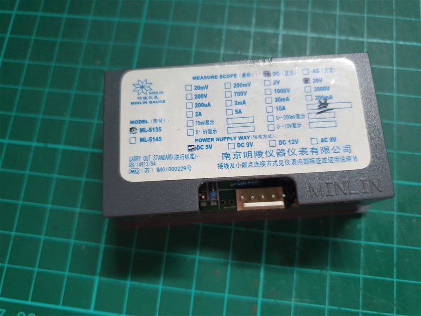
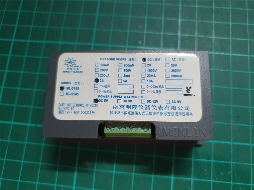
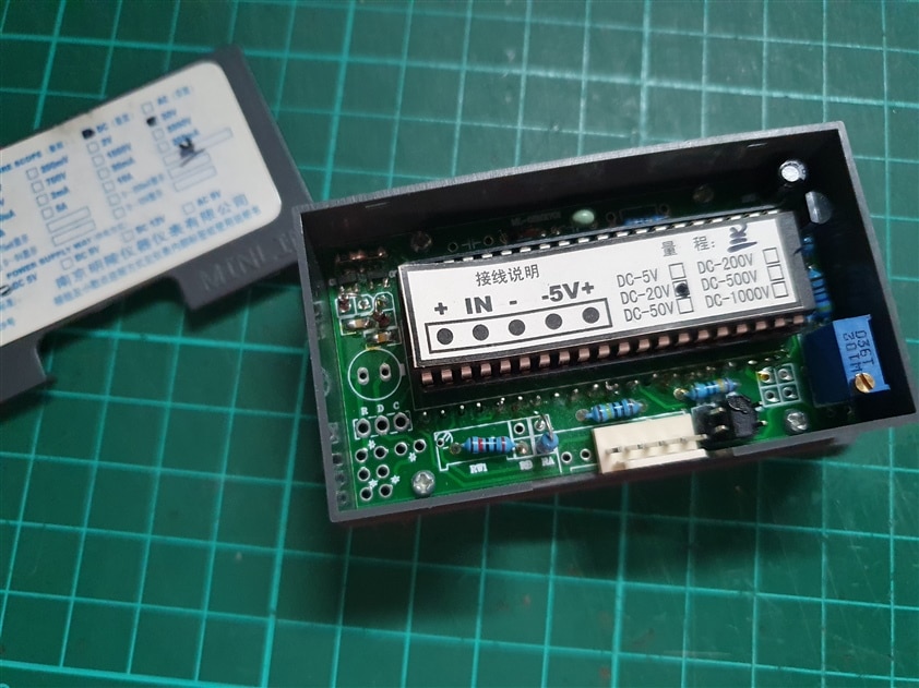
I knew from a distant memory that I had gathered that information when I bought them, but I could not remember it, nor a place where I could have written it down. As a last resort, I decided to delicately pry them open in order to “trace” the pins to whatever is inside. But luck was with me on that one as there is a sticker inside that gives exactly that information:
The only two things left were the PCB itself and the front panel. For the latter, the stars are somewhat aligned as I received a 3D printer as a Christmas gift two years ago and so decided to use it for that.
But for the PCB, I still was in the mood for going the old way with toner transfer and H2O2 + HCl etching. This worked very well for me in the past, albeit on simple circuits. But the traces complexity and the fact that the laser printer is on the verge of dying made me look for other options.
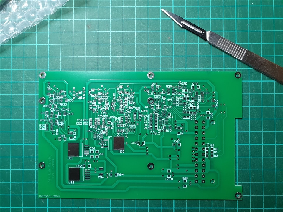
In 2010, that meant paying about 150€ for a custom-made PCB but the landscape has changed quite a lot during the past 15 years and it’s now really cheap to get those online for a tenth of the cost! Here is the board, as produced overseas and sent to me in about 15 days:
Before assembling, and just to get scared, I installed the latest LTSpice version and reran the simulation shown above and… it only gave me flat lines! Let’s hope that’s just a glitch with the new version!
Assembling
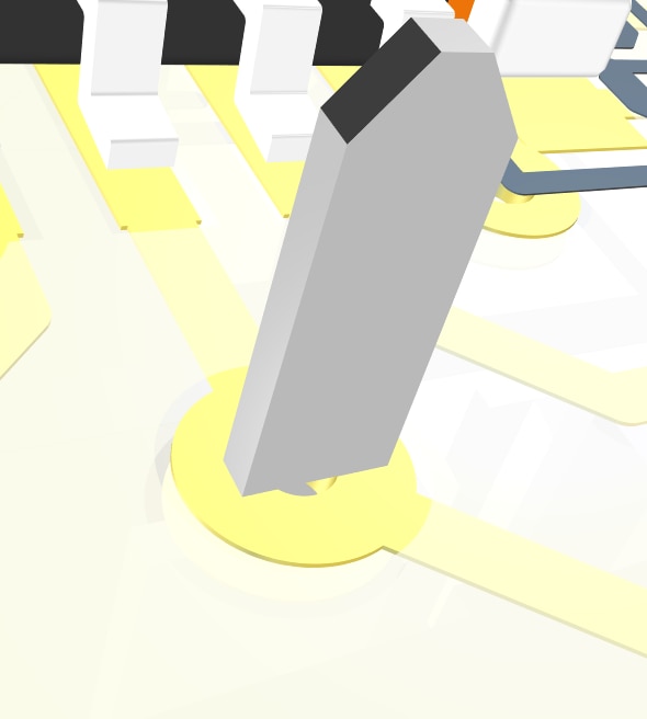
What came up quite early in the assembly phase is that most thru hole pads had a too small opening when compared to what the component itself needed. Some were due to margin errors, but for some, it was definitely a problem between the chair and the keyboard as it was quite clear on the 3D view that it would not fit:
And so here is the first step, redrilling most holes. Sadly, for the potentiometer legs shown above, this meant the pad was completely destroyed in the process! I thus had to expose the copper trace next to them to allow soldering the component, which I did with a fiber glass pen. I had never used such a tool, it’s much easier to use than trying to scrap the protective layer with a scalpel blade.
To make sure I did not forget any holes, I dug up the pack of unused transparent sheets that I used during my student years (twenty-five years ago…) and made a reference that I could place above of the bottom layer.
I then started placing the SMD parts, as shown in this video, played 50 times faster than in reality:
This turned out much easier than I thought, except for the two TSOP6 components, my eyesight has degraded quite a bit in 15 years!
Thru holes components are much easier to install, but it took quite some time as well as can be seen in this sped up video:
Cables are needed to connect the sockets, LEDs and buttons from the board to the front panel:
Yes, I know, those are crimping connectors but I much prefer soldering the cable to the connector on top of crimping them, I do not have great confidence in my crimping tools efficiency, especially on multicore cables.
And with all that, it’s time to construct the front panel. First thing is to add nice looking markings next to each connector. I went with what I have at and, being a laser printer that gave me a nice sheet of paper that I wrapped around the front face and glued in the back:
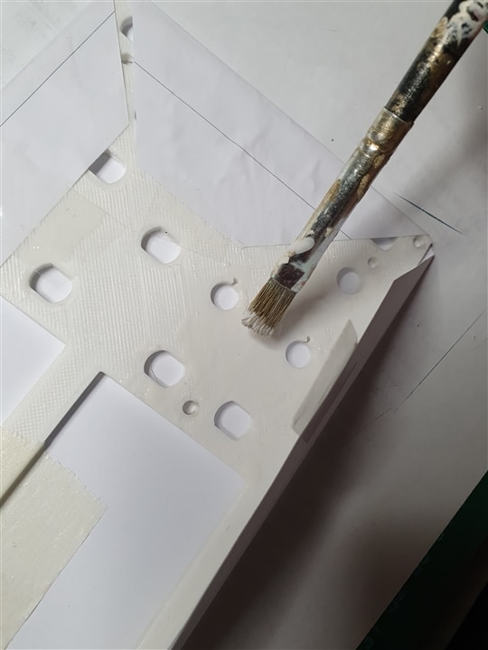
And while the wood glue is drying quite fast, I wanted to make sure it would not come off later on so I sandwiched the panel between two of the five PCB that I ordered and added pressure for a whole night:
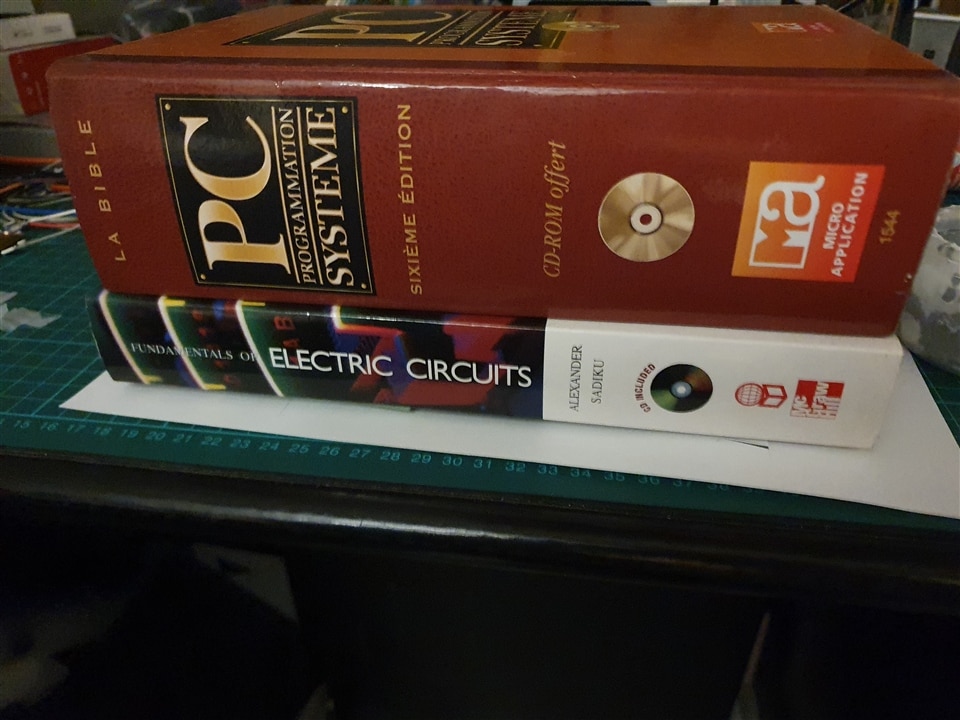
I knew that it was worth keeping those books from my student years!
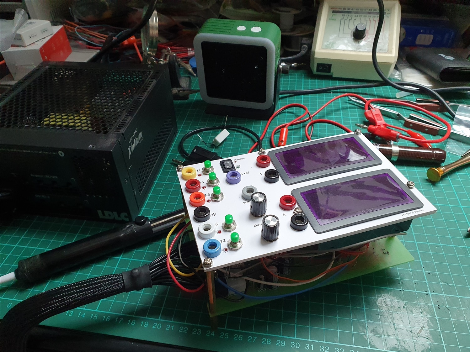
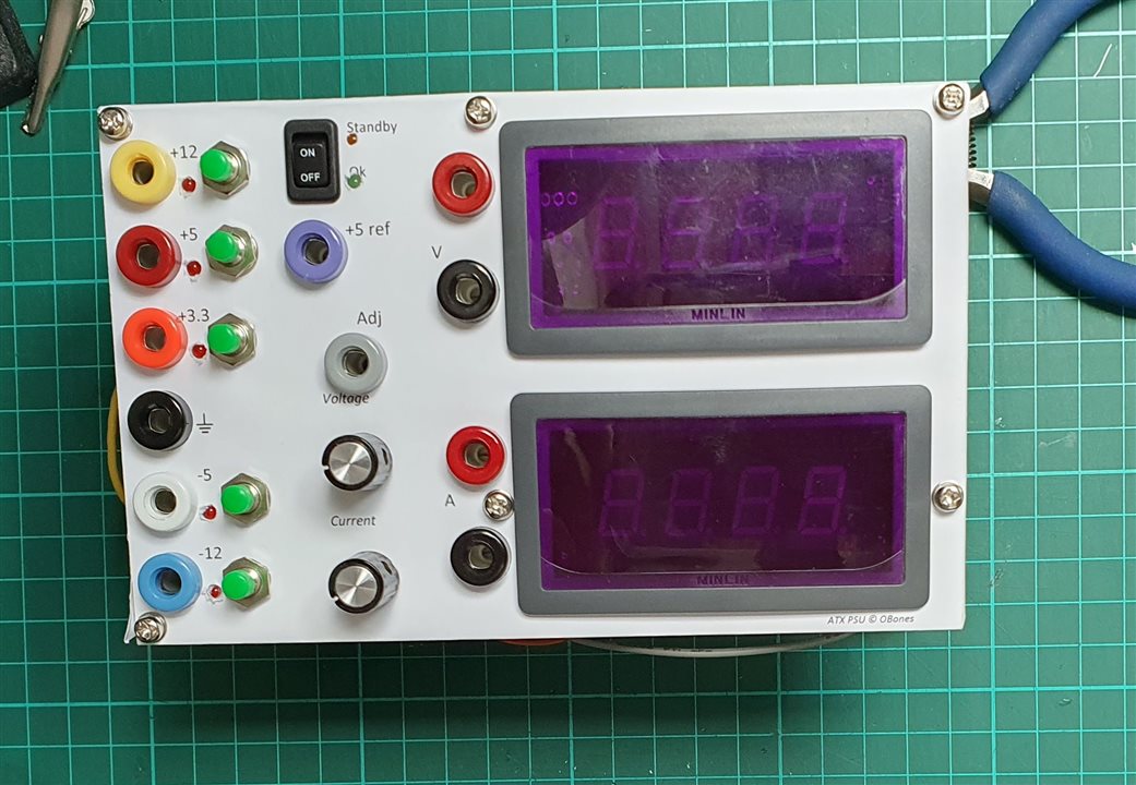
Now, we can place everything on the panel:
In the end, this gives a nice-looking panel:
Powering it up
With everything attached, after a quick check that no power rail is directly touching the GND pins, it’s time to plug the ATX connector and see if this works.
But one thing that came up immediately is that the “male” ATX connector has a detachable 2x2 part with a protruding plastic bit to keep it in place. This is usual on those connectors to be compatible both with ATX20 and ATX24 motherboards, but I did not anticipate it to be so big that it would prevent the connector from fully mating the female part. Running the notch in the PCB up to just beneath the connector would have been a good idea.
Luckily, I had another left over ATX supply where the protruding plastic part is much smaller and was thus able to plug it, turn on the power on the PSU and… it did not go “poof”!
As seen in the video, the -5V fault signal is on but the voltage is still there, meaning that the control circuit for this part is not working.
The voltage and current meters were bought specifically as the “4 wire” versions with the assurance from the seller that they were capable of measuring voltage /current unrelated to their power source. Sadly, this is not the case because leaving the “GND” part floating does not prevent them from working, and we don’t read 7V when using +5 as the reference when measuring the +12V line.
The +5V Ref signal is read as less than +5V when the datasheet says it should be within +- 0.075% to the expected reference, meaning the voltmeter is, unsurprisingly, a bit off in its measurements.
But not all is lost as the adjustable output is working just fine, both in voltage and current mode, as tested with the 50W 3ohms resistor that I had purchased at the same time 15 years ago.
Using the thermal camera from the “Tools and Techniques for Photovoltaic Systems and Solar Arrays” webinar, I can clearly see one hot spot:
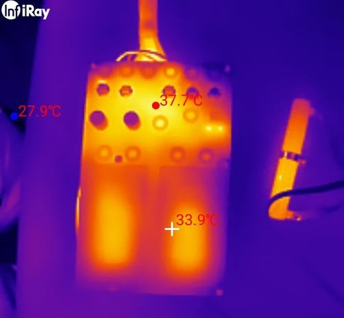
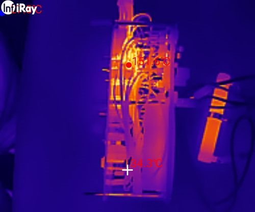
As my office is under the roof and the weather is hot those days, room temperature is at 28°C. But it’s quite obvious the load resistor is very hot, which surprised me as I did not expect the 5W resistor to reach more than 150°C!
In the original order from 15 years ago, I also placed a 3ohms 50W variable resistor to act as a test load. In this thermal video, we can see it heating up when connected to the +5V line, quickly reaching 40°C:
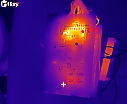
Looking again at the load resistor value, I saw that with 4.7ohms on a 5V line, it meant about 6W going through it, a 20% increase to its rated power. In a stroke of genius, I had also ordered a 27ohms 5W resistor in 2010 and so made a quick replacement. With 5 times less current going through, the dissipated heat is much more manageable.
But after changing that resistor, the over current detection now triggers immediately after startup for +12, +3.3 and -12, and pressing the button does not reset it!
I thought that maybe it was because no current is drawn from those lines on the ATX connector so I added load resistors on those lines specifically:
| Line | Resistor value | Resistor nominal power |
| 12V | 200Ω | 1W |
| 3.3V | 22Ω | 1W |
| -5V | 1kΩ | 1/4W |
| -12V | 2.2kΩ | 1/4W |
Alas, it did not change a thing to the situation, I may end up bypassing my “ocp” circuit altogether.
Conclusion
With about 6 hours assembly time in total, spread in numerous sessions over the course of this past month, I must say that this electronics project has been the biggest I ever undertook.
Add to this the design hours which took place fifteen years ago that would have been well into the 20 to 30 hours range, it’s definitely a bit disappointing that it doesn’t work that well in the end.
But I learnt quite a few things in the process:
- Placing all the orientated capacitors in the same way is a good thing, doing it for connectors as well would have saved time.
- Always double check pad sizes and shapes, even if it’s only on the 3D view. And if possible, make pads a bit larger than required.
- Ensure hole sizes have a bit of margin to account for excess finish that makes them smaller.
- If possible, create a sample circuit before going full size. Yes, the simulation shows that it works, but wasting a few components beforehand can save a bigger waste if the entire board is good for scraps.
- Fiber glass pens are awesome tools when trying to remove varnish from a solid surface.
Even if it was a bit straining on the eyes, I’m quite pleased with myself here and I hope you enjoyed this lengthy report about this fifteen years journey.