


 | Enter Your Electronics & Design Project for a chance to win a Grand Prize for Originality, a Tool Set, and a $100 Shopping Cart! | Project14 Home |
| Monthly Themes | ||
| Monthly Theme Poll |

Introduction
What to do for my Test Instrumentation project? I decided that I'd do a constant-current load but, to be a bit
different, mine doesn't include an op amp to control the loop. Op amps are for wimps - I'm going for the hard stuff
- a transistor design.
Just kidding. Not about the transistors, I am going to use transistors, but if you just want to build a load then
be sensible and use op amps, particularly if you want precision from it. The reason I'm doing it with transistors
is to see what I can manage in the way of a design, putting some of what I've been learning to the test. It's also
going to be a vehicle for looking at more transistor circuit building blocks. Further, I want to see how much speed
I can squeeze out of some very ordinary, low cost, small-signal transistors (2N3904 and 2N3906) along with a
cheapish power MOSFET; just for the challenge of doing it. This one is intended to be a 'speed demon' (maybe),
rather than a slow, ponderous, lumbering beast, which is how many of the op-amp ones seem to end up, so I may well
have some stability issues with it.
Before I started I naively thought I might do something unusual and interesting
with the design but, after I'd been working on it for a while, I discovered I was merely creating a somewhat crude
op amp (slaps head with wet fish). It's not quite a general-purpose op amp, though; it is specific to the job and
differs in some respects from a do-anything device; sometimes for good reason and sometimes out of a general
ignorance as to how these are usually designed. We'll see more of that when I get on to the operation and how it
works, but I'm going to do the build first and show it working in a video because this is also intended to be a
Project14 entry.
Important note: this is an investigation of transistor design techniques and a first prototype of a possible
circuit; it's a long, long way from being a finished project suitable for replication. This may well disqualify me
from the competition and the prizes - I'm not too clear on the rules - but I won't worry at all if it does. (Is that a
strong enough hint for the judges, do you think?).
The Circuit Diagram
Here's the circuit diagram.
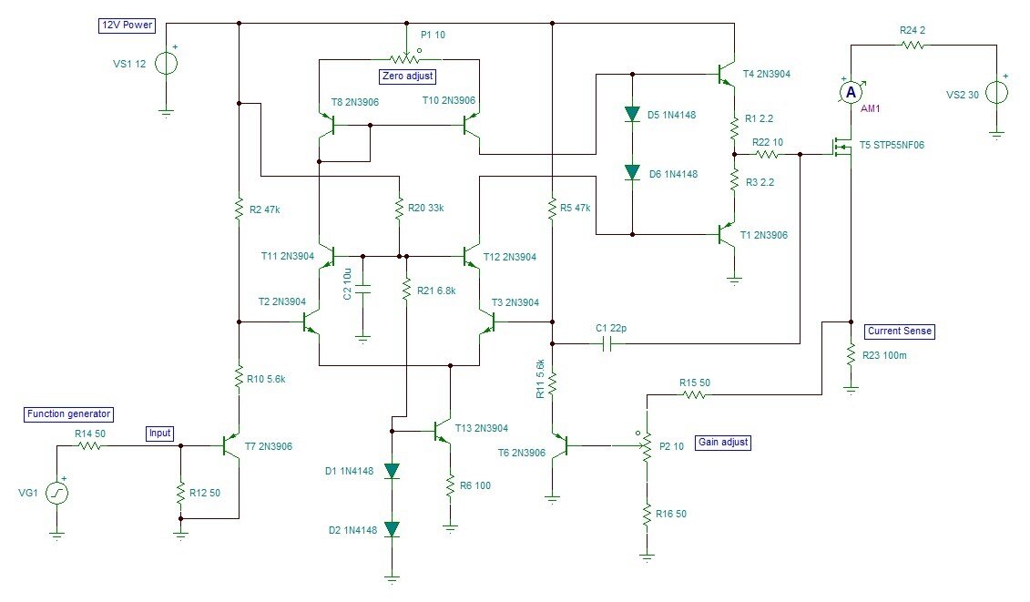
At first glance it will probably look quite complicated - it's also a bit messy because of the way it gradually
developed as I pieced it together in the simulator - but it does neatly break down into distinct, small pieces and
I'll work through the theory of those and the overall operation in a separate blog once I've completed this one to
enter it for the competition. One advantage it has over other circuits is that the build cost of the components is
very low and would probably come in at less than a single precision op amp.
My starting point, as a specification, was that it should equal or better the (very simple) op amp designs in
everything except precision (where I wouldn't stand a chance, even using expensive, specialised matched transistor
arrays and stuff like that) and should run off a single supply (because I like making life difficult for myself -
seriously, if I was doing this design again I'd probably make life easy for myself and go dual-rail; it isn't half
a pain trying to work close to the ground reference). I'm thinking of using this for load testing switching
converters and I wanted an analogue load that could be swept up to frequencies above the bandwidth of the control
loop of the converter to do experiments with (whether that's actually sensible I don't know, but it seems to be
where I'm off to, so best just humour me). In practice, I'm pushing it a bit with these transistors - the 2N3906
only has an fT of 300MHz, though the results in the simulator look reasonable - but if this works ok on a
breadboard (a wired board - I'm not trying it on a plug-in one) I could develop it further with faster devices.
Building the Prototype
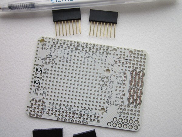
This is the bare prototyping board I'm using. It came in a little bubble pack, with a selection of simple
components, from what was once Maplin Electronics (just before they went into administration). It looks like the
kind of thing that's just bought in and branded, so I imagine it would be very easy to find something comparable.
I'm doing it on an Arduino compatible shield because I may try it with a processor board once I get the load itself
functioning. Then I can make it programmable (more SCPI stuff!).
Here's are pictures of the built prototype, top and bottom.
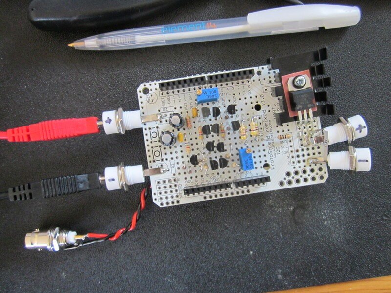
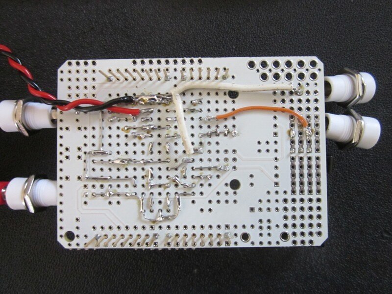
Everything is just soldered in place and the links between components are mostly made with bent over leads, with
the occasional added wire. There's a lot of symmetry in the circuit and that helps with the layout. I've positioned
the power MOSFET at the end where it can be bolted to a heatsink. The load connection and the analogue power (it
needs more than the 5V available from the processor board) are connected with 4mm sockets. I'm not going to fuss
too much over this side of it - it's a prototype and I want to see how well it works, all the miscellaneous stuff
can be tidied up later if I decide to build it into a box. One practical thing I should mention is that I've
matched the transistors for gain, so each transistor down one side of the central column is matched with its
symmetrical partner on the other side. I'm trying to maintain the symmetry as much as possible.
The output circuit I've made as tight a loop as was reasonable on the board. That's to keep the resistances low and
to minimise the inductance as far as possible. The current sense resistor is 100mOhms with a 3W rating and that
will limit me to a (dc) current of 5.47A (probably less, as it has to be derated at temperature). In practice, on
this version built on a circuit board and with only a smallish heatsink for the MOSFET, I'm going to limit it
further and only work up to about 3A, and then only at a duty cycle of less than 100% and with lowish voltages.
(The current sense resistor I've used - an Arcol one - is intended for the function and the spec isn't too bad for
what it cost (about 60p) - 3W, 1%, and 20ppm.)
The MOSFET isn't a 'logic level' part and has a moderately high threshold. That was a deliberate design decision
because it fits nicely with how I'm doing the gate drive. If you did want to experiment with this circuit (without
extensively redesigning it), don't substitute a low-threshold part as it won't work properly. I'm putting this in
as a warning because the ST part I've used also happens to be available in a version with the same part number but
with an L suffix to indicate logic level, so beware.
First Tests
Before I try doing anything with a processor, I'm going to power it up and see how it gets on with a function
generator driving the input. That will allow me to experiment with various waveforms, see how it performs, and get
the zero and gain pots adjusted. If I feed in a square wave, I'll be able to see how the loop responds to a step
change and modify the compensation if it looks either over-damped or under-damped. I chose the capacitor value on
the circuit diagram using the simulator - more on that later - but the real circuit won't match that and it will
probably need some adjustment.
I've now connected it up and put 12V power on it. The supply current is just a few milliamps, so that went ok. I
then connected a bench supply to the load side, set the voltage to 3V so that the MOSFET dissipation wouldn't be
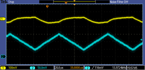
too high, set the function generator to give a triangle wave of 0-500mV and got this (yellow trace is voltage in
from the generator and blue trace is voltage across current sense resistor [100mV = 1A])
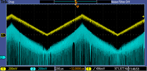
Hmm. That's not too good. The output is oscillating (the disruption to the yellow input trace is probably just
'scope coupling). There's also the mild aroma of a part cooking. That's just the MOSFET warming up, but it's a
reminder that I need to scale back the dissipation a bit - the very small heatsink has it's limits. Powered off,
looked at board and realised I'd left off the compensation capacitor (10pF from the simulation), so that explains the wild
instability.
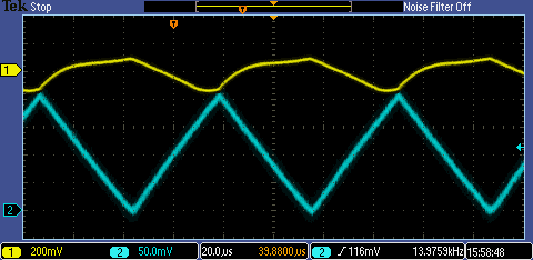
Didn't have a 10pF capacitor, but I've got some 22pF (xtal loads) so I'll use two in series for 11pF.
That deals with most of the oscillation but there's still a problem down near ground. Here's a sine wave and you
can see it's mostly ok but loses it at the bottom where the input just touches 0V. Still, it's quite encouraging
the way the current on the output follows the input voltage.
This next trace shows a tougher test. This is a square wave with fast edges. The output slews nicely, but there's a
fair bit of overshoot and ringing at the top and we can now clearly see the oscillation at the bottom of the range.
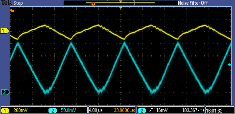
At this point I removed one of the capacitors to give 22pF.
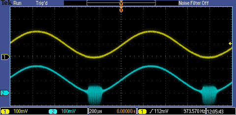
Next is a trace of a triangle wave going in and the current on the output. 200mV on the blue trace is equivalent to
2A and it's following the input quite nicely, though it's only 1kHz.
Now I've gone off at a bit of a tangent (sorry, you know how it is when you're experimenting with things), I'm
testing the power supply connected to the output. The yellow trace on the shot below now shows the voltage of that
supply. That trace has an offset of 3V (the supply voltage) so we can see what happens when the current (the blue
trace) changes. The current is ramping up and down between 0.5A and 1.5A and we can see how the large electrolytic
capacitor on the output of the linear supply behaves.
Here it is again, but with the current ramping up and down between 0A and 2A.
The next one is similar, but the frequency has been increased to about 100kHz. This shows uncertainty at the bottom
when the waveform suddenly changes direction.
The next two traces show a 10kHz sine wave. For the second one, I moved the sine wave down so it was resting on the
0A level. This really emphasises that the problem I have with the oscillation relates to what happens around
ground.


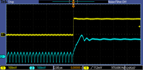
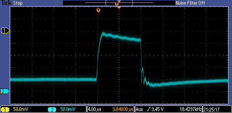
Finally, this is what happens at speed. This is a 0.5A to 2A step up and then back down again 8uS later. This is
with the springy-clip for monitoring the sense resistor rather than the flying ground lead. I didn't try for the
voltage at the same time because of the difficulty of holding both probes in place. That's sort of encouraging
because it does show that the MOSFET can throw the output around pretty fast and the gate drive must be reasonably
good.
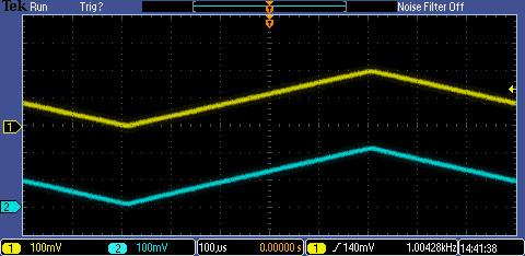
And here it is with a triangle waveform to show that it sort of follows, even at 770kHz, though the gain is rolling
off at that point. I'm back now with the yellow trace showing the input waveform rather than what the PSU on the
output is doing. [The triangle wave from my cheap function generator is a bit embarrassing, isn't it.] However,
that result is somewhat misleading as, in the range between 250kHz and 700kHz, the output does very strange things
and it's only at about 700kHz that it comes right again and starts to follow the input properly again.

One thing that I need to do now is come up with a harder, more solid rail than the output electrolytic in the bench
power supply so that I'm not simultaneously testing the power supply and the load.
That's the point I've reached so far. I haven't met my spec and it isn't a project that you could simply build and
use but, as long as I stay away from 0A on the output, it already has some potential for testing as I've just found
out. For all the problems with it, I'm quite pleased - it's the first thing I've designed with transistors of any
complexity and, though I've pieced it together from thoroughly understood (by people who know what they're doing)
building blocks, it's still neat seeing it there on the bench doing things. The next thing for me to do is to look
in more detail at what the circuit is doing internally and where it differs from the simulation (which is much
better behaved). I'll also go through the design and explain how the circuit works, but I'll blog both of those
separately to this Project14 entry.
The Video
Not much of a video, but it shows the board on the bench and working. Pretend that it's the tidiest bench you've
ever seen.
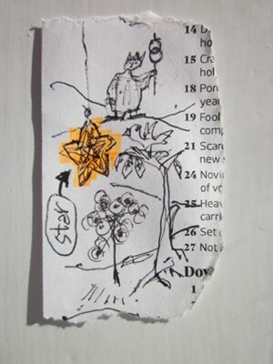
The Doodle
Finally, as a bit of silliness, here's a doodle. This shows the King of the Current Sources who has wandered by and
awarded me one star for my efforts. The bird in the Tree of Knowledge is complaining because he almost hit her on
the head with the star.
Further blogs
Top Comments