Most analog circuits, such as comparators and A/D & D/A converters, need a voltage reference to achieve the desired accuracy and performance. The precision of these circuits depends on a reference that must be independent of manufacturing process tolerances, temperature changes, power supply variations, and more. Primary voltage standards such as the Weston cell are implemented using electrochemical cells or batteries, which have severe limitations in size, cost, complexity, and stability over temperature and time. Advances in precision voltage references have resulted in semiconductor voltage references that can be quite accurate and stable. This learning module covers the essentials of voltage references, focusing on measurement parameters, types, and applications.
2. Objectives
After completing this learning module, you will be able to:
 Understand the basic concepts and operation of a voltage reference
 Explain the different types of voltage references
 Discuss the quality parameters that influence voltage references
 Describe how voltage references are used in different applications
A voltage reference is an electronic circuit or device that ideally produces a constant voltage irrespective of the variation in input and loading on the device. A simple example of a voltage reference is a Zener diode. When current passes through the Zener diode, a voltage develops across its terminals, and as the current continues to increase, this voltage remains relatively constant. This voltage drop depends on the design of the device and materials used. Let us expand our discussion to three different technologies that voltage references are built upon —Zener breakdown, Buried Zener, and bandgap voltage.
- 3.1 Zener-based Voltage Reference
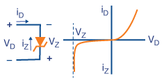
Zener diodes are PN junction diodes with controlled reverse-biased properties, making them useful as voltage reference devices. The V-I characteristics of the ideal Zener diode are shown in Figure 1.
The reverse characteristic shows that, at the breakdown point, the knee voltage (Vz) where the current through the PN junction starts increasing rapidly is relatively independent of the diode current. This knee voltage, also known as Zener voltage, is controlled by the amount of doping applied during the manufacturing process. Practical Zener diodes typically have tolerances of a few percent, so high levels of precision can be difficult to achieve. In addition, while the breakdown voltage is ideally constant as a function of reverse current, in practice this voltage will vary with current, adding further uncertainty to the value. In a simple Zener reference circuit, with the diode driven by a resistor connected to a power supply voltage, the breakdown voltage remains relatively constant as the supply voltage – and therefore the reverse current – varies. If the input voltage increases, the diode maintains a nominally constant voltage across the load by absorbing the extra current and keeping the load current constant. If the load resistance decreases, the current drawn by the Zener diode decreases and the extra current through the load maintains a nominally constant load voltage.
A voltage reference requires stability of the output voltage relative to temperature variations. The Zener voltage varies with temperature, and its variation depends on Zener and avalanche breakdown. The Zener breakdown voltage decreases with the increase in temperature, creating a negative temperature coefficient (NTC). Avalanche breakdown voltage rises with the increase in temperature, creating a positive temperature coefficient. Near 5.6V, the negative temperature coefficient from Zener breakdown is balanced by the positive temperature coefficient from avalanche breakdown, creating a device with a low-temperature coefficient.
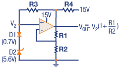
In the manufacturing of a practical Zener-based voltage reference IC, a conventional forward biased diode is used in series with a Zener operating in the avalanche mode to avoid the temperature effect. A forward-biased diode has a negative temperature coefficient, which cancels the positive temperature coefficient of the Zener diode operating in avalanche mode.
A Zener-based voltage reference IC implementation is shown in Figure 2. R4 provides the startup current for the diodes, thus setting the positive input of the op-amp at V2. R3 sets the desired bias current for the diodes. Manufacturers set the output voltage through the ratio of R1 and R2. By trimming these resistors, the output voltage can be set to the desired value. We can optimize bias current to a point where a minimum temperature coefficient is obtained by trimming R3 – but note that any variations in the 15V power supply will affect the current, and therefore the output voltage and the temperature coefficient.
- 3.2 Buried Zener Voltage References
Zener diodes are used to make high-quality voltage references. However, they are very noisy and unstable due to surface impurities and crystal imperfections. In a buried Zener reference, the Zener junction is covered by a protective diffusion below the surface, which makes the device stable and protects it from the noise generated by surface impurities and crystal imperfections.
- 3.3 Bandgap Voltage Reference
A bandgap voltage reference produces the sum of two voltages having opposite temperature coefficients. Similar to Zener-based references, this approach cancels out the temperature effect. Figure 3 shows a bandgap voltage reference circuit where one voltage is the forward voltage (VBE) of the conventional diode (the base-emitter junction) in transistor Q1, which has a negative temperature coefficient; the other is ΔVBE, the difference between the forward voltages of two diodes (the base-emitter junction of Q1 and Q2) with the same current but operating at two different current densities in the ratio of n:1. This is achieved by fabricating Q1 with a larger emitter area than Q2. The negative dependence of VBE is compensated by the positive dependency of ΔVBE and dropped across R1.
Bandgap references typically provide a voltage ranging from 1.2V to 10V. The benefit of bandgap devices is the ability to not only provide reference voltages below 5V but also to enable operating currents down to milliamps and microamps.
We will now discuss different types of commercially available integrated voltage reference devices and their circuit implementations.
- 4.1 Series Voltage Reference
A series voltage reference is a three-terminal device connected in series with its loads, as shown in Figure 4. This mode regulates the output by creating a voltage drop between its input and output. It can be viewed as a voltage-controlled resistance where the output controls an internal resistance between the input and output terminals of the reference device. In the absence of any load, the series reference draws a small amount of current through the internal resistance and drops a voltage between the input and output that is necessary to produce the correct output.
When load current increases, the reference changes its internal resistance to provide the correct voltage drop between the input and output to maintain the specified output voltage.
- 4.2 Shunt Voltage Reference
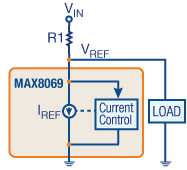
A shunt voltage reference is a two-terminal device connected in parallel with its load, as shown in Figure 5. The complete circuit can be viewed as a voltage-controlled current sink where the controlling voltage is applied to its input terminal. With no load applied, enough current flows through the shunt reference so that the voltage drop across R1 produces the desired output voltage. For example, if the applied input voltage is 8.0V, and the desired reference voltage is 5.0V, the reference IREF creates a 3.0V drop across R1.
When we apply a load to the reference, IREF is not equal to IR1, because load current produces part of the voltage drop across R1. In this case, the reference automatically adjusts its sink current to maintain a constant voltage across the reference. Therefore, the total current through R1 does not change. IR1 is shunted between the reference and load, and hence is called a "shunt reference." A shunt reference controls the output voltage by adjusting its sink current and opposes load current changes.
The units for voltage reference parameters, such as accuracy, differ among manufacturers. Commonly used units of accuracy include parts per million (ppm), the percentage of full scale (%), decibels (dB), and voltage (V/ µV). Let us discuss the relationships for converting one unit to another.
- 5.1 Accuracy Percentage of Full Scale
Percentage of the nominal value is a common means for stating reference accuracy. It follows the convention for expressing tolerance on resistors, capacitors, and inductors. The percent accuracy specifications for voltage references are 1%, 1.5%, 2%, and 5%.
We should multiply the output voltage of the reference device by the percent accuracy and divide by 100 to determine the voltage deviation of a reference. For example, a 3.5V reference accurate to ±1.5% has a deviation of: ± (3.5V × 1.5)/100 = ±0.0525V, or ±52.5mV
- 5.2 Accuracy in Parts per Million
Parts per Million (ppm) is used to specify temperature coefficients and other parameters that change very little under varying conditions. For a 3.5V reference, 1ppm is one-millionth of 3.5V, or 3.5µV. If the reference is accurate to within 10ppm, its output tolerance is: 3.5V × 10/10-6 = 35µV
Conversion in voltage accuracy:
3.5V ± 35µV = 3.499965 V, or 3.500035 V
Conversion in percent:
± (35E - 6V) × 100/3.5V = ±0.001%
- 5.3 Accuracy in Bits
Accuracy in bits is specified as a ± number of bits Least Significant Bit (LSB) or Most Significant Bit (MSB). For example, a 3.5V reference voltage that claims to be 16-bit accurate must not deviate by more than one part in 216 (65536). So, 1 bit is 1/65536 volt of the total voltage value. In this case, it is 3.5/65536 ≈ 53µV. If we consider 1-bit accuracy (±1 LSB), the output voltage can be 1 bit higher or lower than nominal, i.e., ±53µV.
Converting to voltage accuracy:
3.5V ±53µV = 3.499947V, or 3.500053V
Converting to percent:
(±53E - 6V/3.5V) × 100 = ±0.0015%
- 6.1 Initial Accuracy
The initial accuracy of a voltage reference is defined as its worst-case tolerance after the complete production process. We can measure the output voltage of the reference using automatic test equipment (ATE). This specification is generally given for room temperature, with defined load current and input voltage. Package stress can affect the initial accuracy tolerance, so control of the solder temperature profile is required.
- 6.2 Noise
Noise in the reference voltage is a random signal produced by active and passive devices inside the IC. It affects the accuracy. The MAX6250 and MAX6350 are good choices for low noise applications with 3µVp-p noise from 0.1Hz to 10Hz.
- 6.3 Temperature Drift
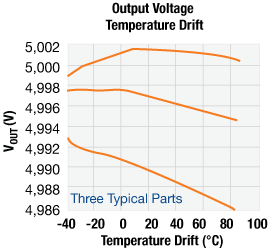
The terms temperature drift and temperature coefficient are generally used interchangeably. Temperature drift is the change in output voltage with regard to temperature and is broadly used to evaluate voltage reference performance. Temperature drift is caused by imperfections and nonlinearities in the circuit elements and specified by ppm/°C. Figure 6 shows how the output of one voltage reference drifts with temperature. The plot below is data for the MAX6005, which is specified as a 100ppm/°C (max) reference.
- 6.4 Thermal Hysteresis
Thermal hysteresis is the change in output voltage when the temperature is cycled - usually between room temperature and the operating temperature limits. As an example, consider a reference that operates over a temperature range of -40°C to +85°C. Thermal hysteresis can be measured by first measuring the output voltage at room temperature (+25°C), then cooling the reference to -40°C, heating it to +85°C, and finally returning it to 25°C. We measure and re-record the output voltage. The temperture hysteresis is the difference in these measurments. This parameter is related to stress on the die. The MAX6001 device is a 3-pin SOT23 with a typical temperature hysteresis of 130ppm. However, a larger, more stable package, like the MAX6190 in the 8-pin SO, has a temperature hysteresis of only 75ppm.
- 6.5 Dropout voltage
Dropout voltage is the difference between input and output voltage that allows the reference to maintain its specified accuracy. It is a critical factor in low-voltage and battery-operated equipment, and applies only to the series reference. Battery voltage decreases with the number of discharges, and the reference must maintain an accurate output voltage by the lowest possible battery voltage to maximize its useful life. Hence, a lower dropout voltage allows continued operation at a lower battery voltage.
- 6.6 Line Regulation
Line regulation is a change in output voltage due to a change in input voltage. It is a DC parameter and is typically specified at DC. It is generally specified by %/V, ppm/V and µV/V of the input voltage. Line regulation is inversely related to the rate at which the line voltage changes, and can be specified by PSRR (power supply rejection ratio). Input capacitors are generally recommended to minimize high-frequency input noise.
- 6.7 Load Regulation
Load regulation is a change in output voltage due to a change in the reference load current, and it is specified by ppm/mA, µA/mA, %/mA or percent change from no load to full load. It includes any self-heating due to power dissipation with load current. This parameter is essential if the reference load current fluctuates while the reference is working, e.g. when a reference drives some types of resistive ladder-type digital-to-analog converter (DAC) with no reference buffer. If the ladder impedance changes significantly with DAC code, the variations in output current can affect the reference’s output voltage. The load regulation is inversely proportional to the rate of change of the load current. There must be output capacitors to stabilize the output voltage.
- 6.8 Line Transient Response
Line transient response is the deviation of the voltage reference output in response to a momentary or transient change in input voltage. For example, a voltage reference can be designed for an output voltage deviation less than 5mV for a 200mV input voltage step in a range of 3.2V to 3.4V in 10 microseconds. It should be noted that the input and output capacitors have a remarkable effect on the performance of the reference.
- 6.9 Load Transient Response
Load transient response, or output settling time, is the response characteristic to an abrupt load variation. It is the time required for the output voltage to return to its specified value after having fallen or risen. Proper capacitor values connected to the reference’s input and output have a significant impact on the performance of the reference.
- 6.10 Turn-on/Turn-off Settling Time
The turn-on settling time is the time to stabilize the output voltage of the reference after an initial power-up. The output is only required to be stable, not necessarily to have reached the specified accuracy. It is dependent on several factors, including the reference’s internal architecture, the input and output capacitor values used, and the applied load. Turn-off settling time is the time for the output voltage of the reference to reach virtually zero volts. This parameter is also dependent on the input and output capacitor values and the applied load.
- 6.11 Long-Term Drift (LTD)
Long-term drift is the variation in output voltage over a long period at some specified condition of steady-state operation. It is a measure of the maximum and minimum output-voltage deviations over an extended period. All other conditions such as temperature, input voltage, and load current must be constant if this measurement is to reflect drift in the reference accurately. It is specified in ppm per 1000 hours.
Many factors can affect a voltage reference's Long-Term Drift, including package stress due to package size, mold compound, PCB stress, and external environmental factors such as temperature and humidity.
The LTD (ppm) can be described by the following function:
LTD (ppm) = f (V, package stress, PCB design, PCB assembly quality, compound settling time, Temperature, humidity)
It is necessary to understand the voltage reference specifications and its contribution to error in order to select the correct reference for the application. Applications such as data acquisition, sensor driving, and comparators need precise voltage references. Let us look at a few design examples.
- 7.1 Data Converters
When used with an ADC or a DAC, the voltage reference determines the input or output range, and therefore has a role in setting the value of the LSB. The digital output of the ADC denotes the ratio of the input voltage and the reference voltage, whereas the digital input to a DAC defines the ratio of its analog output voltage to its reference voltage.
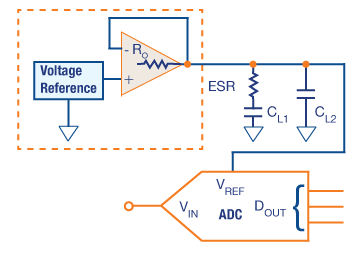
Most data-converters use a sample & hold technique, where a sampling clock processes a large number of equally-spaced analog samples. The quantization value of the analog sample is inversely proportional to the reference voltage. Any instability in the reference will reflect in the precision of the ADC digital value. A voltage reference connected with a successive-approximation-register (SAR) ADC is shown in Figure 7.
- 7.2 Sensors
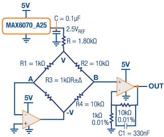
A precise voltage reference is useful for driving some sensor circuits. A voltage reference precisely drives sensors such as resistance temperature detectors, thermistors, or thermocouples in a Wheatstone circuit configuration, which is the first choice for front-end sensors, as shown in Figure 8. A Wheatstone bridge is used to measure an unknown electrical resistance by balancing two legs of the bridge. It has a single impedance-variable element that is inherently nonlinear when away from the balance point.
Since bridge circuits are simple, they are useful for monitoring temperature, pressure, humidity, light, and other analog properties in industrial and medical applications.
- 7.3 Comparators
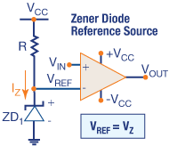
A voltage reference is used with comparators to make a precise and accurate set trip point. A comparator circuit with Zener voltage reference is shown in Figure 9. The behavior and accuracy of the comparator circuit depends highly on the voltage reference. Comparators are widely used in ADC, level detection, Schmitt triggers, clock-recovery circuits, window detectors, and on-off controls.
Voltage references form significant circuit blocks in systems such as data conversion systems, power supply monitors, test instruments, and sensor drivers. Let us look at some applications of Voltage reference ICs designed by Maxim.
- 8.1 Analog Current/Voltage Output for Industrial Automation and Control
The Carmel subsystem reference design board, shown in figure 10, is an analog current/voltage output board that uses a MAX6126 voltage reference IC. This IC features curvature-correction circuitry and high-stability, laser-trimmed, thin-film resistors that result in 3ppm/°C (max) temperature coefficients and ±0.02% (max) initial accuracy. This design board is suitable for programmable logic controllers (PLCs), distributed control systems (DCSs), and other industrial applications to produce voltages and currents.
- 8.2 Simple Power Monitor using MAX6025A, SOT23-3 Voltage References
The power monitoring circuit is used to monitor a system supply voltage. It is implemented using a MAX6025, which is a low power, low-dropout voltage reference IC. This circuit allows an ADC to monitor the system supply voltage through the reference input of the ADC.
Power monitor circuits often use a reference voltage that is lower than the supply voltage. An external resistor-divider may be used to decrease the voltage applied to the ADC input, but external resistors produce errors that may be objectionable in many applications. The modified circuit shown in Figure 11 eliminates the voltage divider, and applies the supply voltage directly to the ADC’s reference input. In this case, the ADC must be capable of accepting an external reference as high as the supply voltage, which is a common feature of most general-purpose ADCs.
- 8.3 4-20mA Input Isolated Analog Front End (AFE) for Industrial Sensor and Process Control
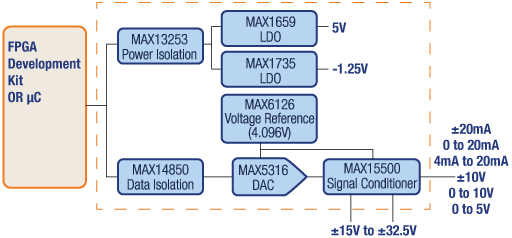
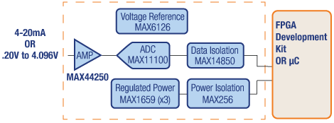
The Campbell (MAXREFDES4#) subsystem reference design, as shown in Figure 12, is mainly targeted for industrial sensors, automation, process control, programmable logic controllers (PLCs), and medical applications where a 16-bit high-accuracy industrial analog front end (AFE) is required. It accepts a 4–20mA current loop or a 0.2V-to-4.096V voltage input signal and features isolated power and data. The Campbell design integrates an ultra-high-precision 4.096V voltage reference (MAX6126), a precision low-noise buffer (MAX44250), 600VRMS data isolation (MAX14850), a high-accuracy ADC (MAX11100), and isolated/regulated 5V power rails (MAX256/MAX1659).
- 8.4 Application of LM404 in Base Station
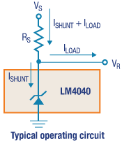
The power amplifier (PA) system is one of the critical components in a Base station for wireless communications. The PA system performance is optimized by combining components such as an ADC, DAC, temperature sensor, a current sense amplifier, precision reference voltage, and a microcontroller unit as shown in Figure 13. The accuracy and performance of all components are highly dependent on the voltage reference block used.
The LM4040 is a precision, two-terminal shunt mode, bandgap voltage reference. It is available in fixed reverse breakdown voltages of 2.048V, 2.500V, 3.000V, 3.3V, 4.096V, and 5.000V. The Laser-trimmed resistors ensure precise initial accuracy. With a 100ppm/°C temperature coefficient, the device has four grades of initial accuracy ranging from 0.1% to 1%. There is no capacitor required on the output, and it ensures stability with any capacitive load and operates over the temperature range of -40°C to +125°C.
Figure: 13: Current Monitoring and Control in the PA System and LM4040 Operating Circuit
- 8.5 80mA Precision Reference
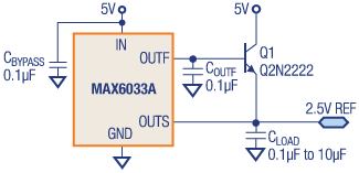
Large systems with many loads on the reference voltage may require more current than the voltage reference IC is capable of sourcing. A buffer circuit at the reference-IC output is a standard solution, but the offset voltage of the buffer tends to decrease reference accuracy. A better solution is to incorporate the buffer inside the feedback loop of the reference error amplifier. The MAX6033A voltage reference, as shown in Figure 14, offers output force and sense pins for this purpose. This device features a SOT23 package, 0.04% initial accuracy, and a 7ppm/°C temperature coefficient.
The power dissipation limit of the output transistor restricts the output current to 80mA.
*Trademark. Maxim Integrated is a trademark of Maxim Integrated Inc. Other logos, product and/or company names may be trademarks of their respective owners.

Shop our wide range of voltage references, including series, shunt, fixed, or adjustable, evaluation boards, and other accessories.
Test Your KnowledgeBack to Top
Are you ready to demonstrate your Voltage Reference knowledge? Then take a quick 15-question multiple choice quiz to see how much you've learned from this learning module.
To earn the Voltage Reference Badge, read through the module, attain 100% in the quiz at the bottom, leave us some feedback in the comments section, and give the module a star rating.








Top Comments