element14 Community
element14 Community
    Register Log In
  • Site
  • Search
  • Log In Register
  • Community Hub
    Community Hub
    • What's New on element14
    • Feedback and Support
    • Benefits of Membership
    • Personal Blogs
    • Members Area
    • Achievement Levels
  • Learn
    Learn
    • Ask an Expert
    • eBooks
    • element14 presents
    • Learning Center
    • Tech Spotlight
    • STEM Academy
    • Webinars, Training and Events
    • Learning Groups
  • Technologies
    Technologies
    • 3D Printing
    • FPGA
    • Industrial Automation
    • Internet of Things
    • Power & Energy
    • Sensors
    • Technology Groups
  • Challenges & Projects
    Challenges & Projects
    • Design Challenges
    • element14 presents Projects
    • Project14
    • Arduino Projects
    • Raspberry Pi Projects
    • Project Groups
  • Products
    Products
    • Arduino
    • Avnet Boards Community
    • Dev Tools
    • Manufacturers
    • Multicomp Pro
    • Product Groups
    • Raspberry Pi
    • RoadTests & Reviews
  • Store
    Store
    • Visit Your Store
    • Choose another store...
      • Europe
      •  Austria (German)
      •  Belgium (Dutch, French)
      •  Bulgaria (Bulgarian)
      •  Czech Republic (Czech)
      •  Denmark (Danish)
      •  Estonia (Estonian)
      •  Finland (Finnish)
      •  France (French)
      •  Germany (German)
      •  Hungary (Hungarian)
      •  Ireland
      •  Israel
      •  Italy (Italian)
      •  Latvia (Latvian)
      •  
      •  Lithuania (Lithuanian)
      •  Netherlands (Dutch)
      •  Norway (Norwegian)
      •  Poland (Polish)
      •  Portugal (Portuguese)
      •  Romania (Romanian)
      •  Russia (Russian)
      •  Slovakia (Slovak)
      •  Slovenia (Slovenian)
      •  Spain (Spanish)
      •  Sweden (Swedish)
      •  Switzerland(German, French)
      •  Turkey (Turkish)
      •  United Kingdom
      • Asia Pacific
      •  Australia
      •  China
      •  Hong Kong
      •  India
      •  Korea (Korean)
      •  Malaysia
      •  New Zealand
      •  Philippines
      •  Singapore
      •  Taiwan
      •  Thailand (Thai)
      • Americas
      •  Brazil (Portuguese)
      •  Canada
      •  Mexico (Spanish)
      •  United States
      Can't find the country/region you're looking for? Visit our export site or find a local distributor.
  • Translate
  • Profile
  • Settings
Essentials
  • Learn
  • Learning Center
  • Essentials
  • More
  • Cancel
Essentials
Documents Related Components for element14 Essentials: Semiconductors I
  • Forum
  • Documents
  • Polls
  • Files
  • Members
  • Mentions
  • Sub-Groups
  • Tags
  • More
  • Cancel
  • New
Essentials requires membership for participation - click to join
Actions
  • Share
  • More
  • Cancel
Engagement
  • Author Author: pchan
  • Date Created: 24 Nov 2020 9:13 PM Date Created
  • Last Updated Last Updated: 8 Dec 2020 5:36 PM
  • Views 704 views
  • Likes 0 likes
  • Comments 0 comments
Related
Recommended

Related Components for element14 Essentials: Semiconductors I

element14 Learning Center


image

Semiconductors I: GaNFETs for Power Conversion

Sponsored byimage


The element14 Essentials of GaN FETs for Power Conversion covers the requirements of electronics in power conversion applications, the limitations of current solutions, and the potential for GaNFETs (Galium-Nitride Field Effect Transistors). To extend the knowledge covered in the main module, this supplementary guide discusses the types of related components used for prototyping or product development.

Go to Learning Module


Components


image

GAN063-650WSAQ Gallium Nitride (GaN) Transistor, Gan FET, 650 V, 34.5 A, 0.06 ohm, 15 nC, TP-247, Through Hole

Buy NowBuy Now

The GAN063-650WSA is a 650 V, 50 mΩ Gallium Nitride (GaN) FET. It is a normally-off device that combines Nexperia's state-of-the-art high-voltage GaN HEMT and low-voltage silicon MOSFET technologies—offering superior reliability and performance. AEC-Q101 qualified.

image Ultra-low reverse recovery charge

image Simple gate drive (0 V to +10 V or 12 V)

image Robust gate oxide (±20 V capability)

image Ultra-low reverse recovery chargeHigh gate threshold voltage (+4 V) for very good gate bounce immunity

image Very low source-drain voltage in reverse conduction mode

image Transient over-voltage capability (800 V)

image AEC-Q101 qualified


image

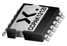
GAN039-650NTB 650 V, 33 mOhm Gallium Nitride (GaN) FET in a CCPAK1212i package

Buy Now

The GAN039-650NTB is a 650 V, 33 mΩ Gallium Nitride (GaN) FET in a CCPAK1212i inverted package. It is a normally-off device that combines Nexperia's latest high-voltage GaN HEMT H2 technology and low-voltage silicon MOSFET technologies—offering superior reliability and performance.

Simplified driver design, as standard level MOSFET gate drivers can be used:

image 0 V to 12 V drive voltage

image Gate threshold voltage VGSth of 4 V

image Robust gate oxide with &plsumn;20 V VGS rating

image High gate threshold voltage of 4 V for gate bounce immunity

image Low body diode Vf for reduced losses and simplified dead-time adjustments

image Transient over-voltage capability for increased robustness

CCPAK package technology:

image Improved reliability, with reduced Rth(j-mb) for optimal cooling

image Lower inductances for lower switching losses and EMI

image 175°C maximum junction temperature

image High Board Level Reliability absorbing mechanical stress during thermal cycling, unlike traditional QFN packages

image Visual (AOI) soldering inspection, no need for expensive x-ray equipment

image Easy solder wetting for good mechanical solder joints


image

GAN039-650NBBA 650 V, 33 mOhm Gallium Nitride (GaN) FET in a CCPAK1212 Package

Buy Now

The GAN039-650NBBA is an Automotive qualified 650 V, 33 mΩ Gallium Nitride (GaN) FET in a CCPAK1212 package. It is a normally-off device that combines Nexperia's latest high-voltage GaN HEMT H2 technology and low-voltage silicon MOSFET technologies—offering superior reliability and performance. This product has been fully designed and qualified to meet AEC-Q101 requirements.

Fully automotive qualified to AEC-Q101:

image 175°C rating suitable for thermally demanding environments

Simplified driver design, as standard level MOSFET gate drivers can be used:

image 0 V to 12 V drive voltage

image Gate threshold voltage VGSth of 4 V

image Robust gate oxide with &plsumn;20 V VGS rating

image High gate threshold voltage of 4 V for gate bounce immunity

image Low body diode Vf for reduced losses and simplified dead-time adjustments

image Transient over-voltage capability for increased robustness

CCPAK package technology:

image Improved reliability, with reduced Rth(j-mb) for optimal cooling

image Lower inductances for lower switching losses and EMI

image 175°C maximum junction temperature

image High Board Level Reliability absorbing mechanical stress during thermal cycling, unlike traditional QFN packages

image Visual (AOI) soldering inspection, no need for expensive x-ray equipment

image Easy solder wetting for good mechanical solder joints


image

GAN041-650WSB 650 V, 35 mΩ Gallium Nitride (GaN) FET in a TO-247 package

Buy Now

The GAN041-650WSB is a 650 V, 35 mΩ Gallium Nitride (GaN) FET in a TO-247 package. It is a normally-off device that combines Nexperia's latest high-voltage GaN HEMT H2 technology and low-voltage silicon MOSFET technologies—offering superior reliability and performance.

image Ultra-low reverse recovery charge

image Simple gate drive (0 V to +10 V or 12 V)

image Robust gate oxide (±20 V capability)

image High gate threshold voltage (+4 V) for very good gate bounce immunity

image Very low source-drain voltage in reverse conduction mode

image Transient over-voltage capability


image

GAN039-650NBB 650 V, 33 mOhm Gallium Nitride (GaN) FET in a CCPAK1212 Package

Buy Now

The GAN039-650NBB is a 650 V, 33 mΩ Gallium Nitride (GaN) FET in a CCPAK1212 package. It is a normally-off device that combines Nexperia's latest high-voltage GaN HEMT H2 technology and low-voltage silicon MOSFET technologies—offering superior reliability and performance.

Simplified driver design, as standard level MOSFET gate drivers can be used:

image 0 V to 12 V drive voltage

image Gate threshold voltage VGSth of 4 V

image Robust gate oxide with ±20 V VGS rating

image High gate threshold voltage of 4 V for gate bounce immunity

image Low body diode Vf for reduced losses and simplified dead-time adjustments

image Transient over-voltage capability for increased robustness

CCPAK package technology:

image Improved reliability, with reduced Rth(j-mb) for optimal cooling

image Lower inductances for lower switching losses and EMI

image 175°C maximum junction temperature

image High Board Level Reliability absorbing mechanical stress during thermal cycling, unlike traditional QFN packages

image Visual (AOI) soldering inspection, no need for expensive x-ray equipment

image Easy solder wetting for good mechanical solder joints


*Trademark. Nexperia is a trademark of Nexperia Inc. Other logos, product and/or company names may be trademarks of their respective owners.

  • ganfet
  • nexperia
  • semiconductors
  • essentials
  • gan
  • power_conversion
  • Share
  • History
  • More
  • Cancel
  • Sign in to reply
element14 Community

element14 is the first online community specifically for engineers. Connect with your peers and get expert answers to your questions.

  • Members
  • Learn
  • Technologies
  • Challenges & Projects
  • Products
  • Store
  • About Us
  • Feedback & Support
  • FAQs
  • Terms of Use
  • Privacy Policy
  • Legal and Copyright Notices
  • Sitemap
  • Cookies

An Avnet Company © 2025 Premier Farnell Limited. All Rights Reserved.

Premier Farnell Ltd, registered in England and Wales (no 00876412), registered office: Farnell House, Forge Lane, Leeds LS12 2NE.

ICP 备案号 10220084.

Follow element14

  • X
  • Facebook
  • linkedin
  • YouTube