


DC Power I: DC-to-DC Converters
Sponsored by

DC-to-DC converters yield precise, constant, and regulated power to various devices, circuits, and appliances. They offer different voltage and power levels to GPUs, CPUs, SoCs, and ASICs used in diverse applications, such as servers, datacom, storage, consumer, and telecom. These converters also find popular use in battery-operated electronic devices such as cellular phones and laptop computers. Based on a new Source-Down technology, a wide range of DC-to-DC converters and MOSFETs, including those with integrated power stages, multi-phase digital controllers, and integrated POL converters are available to achieve the best outcomes. This learning module will discuss some of these converters, the DC-to-DC converter's basic concepts, and use case applications.
2. Objectives
Upon completion of this module, you will be able to:
 Explain the basic concepts, topologies, and key characteristics of DC-DC converters
Understand Source-Down technology and its benefits
Discuss different power converter devices and use cases offered by Infineon
A DC-to-DC converter is a circuit in a power supply that converts a DC voltage level to another DC voltage level. They are classified into two types: linear and switched. Linear DC-DC circuits use linear regulators (LDOs), which function on the concept of a resistive voltage dip to generate and control a particular output voltage. Switched-mode converters are based on the idea of periodically storing the input energy either in an inductor, transformer, any magnetic field component, or in an electric field component like a capacitor, and then releasing it to the output at a different voltage. A closed feedback loop is used to maintain constant voltage output with varying input voltages and output loads. Switched-mode DC-DC is further classified into the categories of isolated and non-isolated converters. Figure 1 shows a simple DC-DC converter circuit with a linear regulator and a switched-mode regulator.


Figure 1: Linear Regulator and Switched-Mode (Buck) DC-DC Converter
DC-DC converters produce output either lower or higher than the input voltage, and are mainly categorized into three conversion topologies: Buck, Boost, and Buck-Boost.
- 3.1 Buck Converter Topology

Figure 2: Buck Converter circuit
A buck converter generates a lower output voltage than the input voltage, and is termed a "step-down" converter. This DC-DC conversion is non-isolating, meaning that there is a common ground between input and output. Figure 2 shows a simple circuit of a buck DC-DC converter. When switch S is on, energy is stored in inductor L as the current flows to the load, and capacitor C is charged. When S is off, the inductor releases the stored energy. The current flows into the load and circulates via diode D, and Capacitor C provides energy to the load. High-frequency switching produces an output proportional to the duty cycle. The switch and the diode shown in the figure are FETs, used as synchronous rectifiers to reduce losses and improve efficiency.
- 3.2 Boost Converter Topology

Figure 3: Boost Converter Circuit
Boost converter topology produces a higher voltage than the input voltage, and is also called a step-up converter. Figure 3 shows an elemental boost DC-DC converter circuit. With switch S turned on, the current flows through the inductor L, returning to input via switch S. The inductor stores the energy during this period. With transistor S off, the inductor functions akin to a voltage source in series with the input voltage. The inductor's stored energy is circulated via diode D to load, and this charges capacitor C to a higher level than the input voltage. The on-time of switch S defines the output voltage.
- 3.3 Buck-Boost Converter Topology

Figure 4: Buck-Boost Converter
A Buck-Boost converter is a combination of buck and boost circuits, as shown in figure 4. In this topology, the converter output voltage can be higher or lower than the input voltage. S2, L, and D2 make the boost converter work when switch S1 is on. Switch S1, L, and D1 make the buck circuit and work when S2 is off.
- 3.4 Key Parameters and Selection Criteria
A DC-DC converter must operate within the required DC parameters, such as the specified input voltage range, the output voltage range, and the maximum current of output needed for a particular application. The other performance parameters that must be considered are efficiency, output ripples, load regulation, transient response, temperature rating, size, and weight. The switching frequency is another critical parameter that affects efficiency and noise. Higher switching frequency allows smaller external components and lower peak currents and I2R losses, but it also increases core losses, gate-charge currents, and switching losses.
To select the DC-DC converter's peripheral components, we should check the datasheet to ensure each component's suitability for the application. The inductor is determined based on inductance value, DC resistance (DCR), the peak current requirement, and the desired switching frequency. The input capacitor minimizes both peak current extracted from the input supply, and the radiated noise to all other system elements. Ensure that the capacitor has a ripple-current rating proximate to the chosen switching frequency.
- 3.5 Range of DC-DC Converters and MOSFETS
OptiMOS Power MOSFET Source-Down
The OptiMOS Power MOSFET Source-Down introduced by Infineon comes in an enhanced PQFN package, and is available in Source-Down Center-Gate (optimized for paralleling) and Source-Down versions. The new Source-Down technology has the silicon inverted within the component and offers better thermal performance and lower RDS(on) performance compared to alternative solutions. IQE006NE2LM5, IQE006NE2LM5CG, IQE013N04LM6CG, and IQE013N04LM6 are a few examples from Infineon's OptiMOS Source-Down portfolio. All of these are low-voltage power MOSFETs included in the PQFN 3.3x3.3 Source-Down package. They are commonly used in drives, telecom, SMPSs, and servers.
Power Management ICs (PMICs)
Infineon's power management ICs comprise tightly integrated OPTIREG and PMBus power management ICs. They monitor, sequence, and execute functional safety support, simplifying design and preserving board space. PMICs are scalable, efficient solutions for multiple applications in the industrial and automotive fields.
OPTIREG PMICs offer integrated, multi-rail power supply solutions for demanding automotive environments. They contribute productive, efficient voltage regulation, including pre-and post-regulator architectures with DC-DC, linear, and tracking regulators. Supervisory features allow automotive ECU design for safety-relevant applications.
The PMBus PMIC comes with standard PMBus commands, which offer an easy-to-use interface for status and telemetry. It can configure output voltages in 5 mV steps, and a five output Point of Load (POL) digital voltage regulator for FPGAs, ASICs, and other multi-rail power systems. Additional applications comprise CPU multi-rail systems, embedded computing systems, storage systems, and communication.
Switching Regulators
Infineon's Switching Regulators include switching regulators for industrial applications and OPTIREG Switchers for automotive applications. OPTIREG Switchers endure harsh automotive environments and provide a dedicated feature set to design effective automotive ECUs. The integrated power stages, soft-start feature, and integrated compensation network reduce the needed amount of external components, system costs, and board space. They offer low current consumption in PFM mode at light loads, to optimize efficiency. The switchers detect under-voltage and overvoltage conditions of the output voltage and indicate the same with the reset output signal. The integrated thermal shutdown feature secures the device from overheating.
Industrial Switching regulators span a broad range of industrial, communication, consumer, and multi-market applications. High-efficiency switching DC-DC converters reduce energy consumption, lengthen battery-powered systems' operational life, and minimize system operating costs.
Integrated POL (Point-of-Load) Voltage Regulators
The Integrated POL Voltage Regulators portfolio from Infineon includes Integrated POL Analog Voltage Regulators and Integrated POL Digital Interfaces. The POL converters consolidate a PWM controller, driver, and MOSFETs into a compact, easily usable PQFN package. The patented PWM modulation scheme permits more than 1 MHz switching frequencies to deliver ultra-compact layouts and the smallest bill-of-materials within -40° to 125°C operating temperatures. They feature essential protection functions like pre-bias startup, internal soft-start, hiccup overcurrent protection, and thermal shutdown to provide the needed system-level security during fault conditions.
The digital interface IPOL devices are unified, and the capable DC regulator provides I2C/PMBus, Parallel VID, and Intel SVID.
DC-DC converters are a crucial component of almost all electronic circuits where different voltages are needed to power diverse circuit components. We will analyze the new Source-Down package innovation and use-case applications using Infineon DC-DC converters and power MOSFETs.
- 4.1 Source-Down Technology
In the Source-Down package, the silicon die is placed inverted inside the MOSFET package. The source potential is attached to the lead frame instead of the drain potential. The silicon gate and source connection of the silicon die are directly connected onto the lead frame, as shown in Figure 5 (on the right). A large copper clip connects the drain from the top. The drain, source, and gate connections remain in the same location as standard PQFN 3.3x3.3 devices, making a drop-in replacement extremely easy.


Figure 5: Internal construction of a PQFN 3.3x3.3 mm Drain-Down power MOSFET (left) and Source-Down power MOSFET (right)
- 4.2 Source-Down Benefits
The new Source-Down footprints come with several benefits: improved RDS(on), optimized thermal management capabilities, and parallel operation, as described in the following content.
RDS(on): Inverting the die eliminates a few construction limitations. The Source-Down approach relaxes some constraints and enables larger dies, and reduces RDS(on) by 30% compared to a standard MOSFET. Lower RDS(on) is directly linked to the reduction of I2R losses in the application, and leads to greater power densities. It is now possible to replace a Super SO8 (30mm2 PCB area) with a Source Down in PQFN 3.3 x 3.3 (10 mm2), resulting in improved performance.
Thermal Management Optimization: The Source-Down package optimizes parallel operation and thermal management. In applications where the drain is connected to the switched node, like in a buck converter or synchronous rectifiers on the SMPS's secondary side, it is inadvisable to connect the drain pad to a large copper area heatsink. In this case, the sole technique to eliminate losses is via a source copper clip and then to the ground plane, as shown in Figure 6. With Source-Down, the thermal management in ground-referenced set-ups is much easier. The source can be connected to all ground planes using thermal vias, resulting in an improved heat transfer to the ambient.


Figure 6: Thermal management with "Drain Down" (left) and "Source Down" (right)
Paralleling Made Easy: Higher current capability can be achieved by paralleling devices. With Drain-Down, the distance from drain to source is inadequate to route the gate signal under the device; another PCB layer must connect the gates, as shown in Figure 7. The Center-Gate variant, with its 0.75mm creepage distance (drain to source), offers the possibility to route the gate signal of paralleled devices sans another layer.


Figure 7: Paralleling with "Drain Down" (left) and "Source Down" (right).
Applications Benefits of the Source-Down package: The low RDS(on) of the Source-Down benefits applications like e-fuses or ORings. Even with a high current of 30A, the Source-Down remains cool at 40.2°C, which results in better reliability and fewer parts in parallel.
Source-Down enhances synchronous rectifier design on an SMPS's secondary side. The switches are generally ground-referenced, as shown in Figure 8.


Figure 8: Multiple ground-referenced MOSFET
Source-Down optimizes thermal management in buck converters and other half-bridge configurations. Figure 9 illustrates a Drain-Down being used as the high-side and a Source-Down as the low-side switch. Both devices are now linked to big copper areas. The switch node may disconnect from the large copper area, avoiding possible EMI issues.


Figure 9: Buck converter with a Drain Down/Source Down combination
- 4.3 Applications
The following are a few application examples using these low-voltage power MOSFETs and DC-DC converters.
Powered Tools with OptiMOS Source-Down 40 V (IQE013N04LM6): Infineon's IQE013N04LM6 1.35 mΩ, 40 V MOSFET in a 3.3x3.3 PQFN Source-Down package (also available in a Center-Gate version) defies the status quo in form factor and power density in end applications. In power tools, it minimizes the PCB's internal space, enabling an ergonomic tool design. Since the design goal is to achieve the smallest possible form factor of the motor drive circuit, a MOSFET case temperature of ~100°C is permissible under full load. This new IQE013N04LM6 achieves high performance at 400 W of maximum power with an optimized form factor, while meeting the design requirements. Figure 10 shows a block diagram of a battery-powered motor using OptiMOS Source-Down low-voltage power MOSFETs.
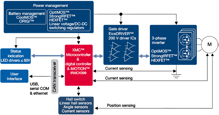
Figure 10: Battery Powered Motor Control
Computing and Data Storage with OptiMOS IPOL Buck Regulators: Energy efficiency and costs are a major concern when it comes to computers and data storage. The total system comprises numerous chipsets, such as GPUs, storage controller ICs, CPUs, and memory. All of these can be powered with the OptiMOS IPOL Buck regulator. This application illustrates the use of OptiMOS IPOL Buck regulators, such as the IR3889 series, operated with a single supply. It utilizes a fast Constant On-Time (COT) control scheme to achieve an accelerated control response. It has programmable switching frequency, selectable current limits, selectable soft-start times, Forced Continuous Conduction Mode (FCCM), and Diode Emulation Mode (DEM) operation. Figure 11 shows a system block diagram of a computing and data storage system with this converter IC's application circuit.


Figure 11: Computing and Data Storage Block Diagram with IR3889 Application Circuit
Glossary
Output Ripple: small variations in output voltage. Many circuits are extremely sensitive to any noise on their input supply, so a small amount of ripple in the output voltage is to be expected.
Current Output: the maximum current a voltage regulator can offer. It depends on the internal power transistor's current-carrying capability.
Noise: random fluctuations in the output voltage generated by components like transistors and resistors.
Load Regulation: the regulator's ability to maintain output voltage steadily during load current fluctuation.
Load Transient: the response of the output voltage to an unexpected step-change in load current.
Line Transient: the response of the output voltage to unforeseen step-changes in the input voltage.
Line Regulation: measures variation in the regulator's output voltage due to input variations.
Efficiency: a measure of wasted power by the regulator. A linear regulator has lower efficiency, as it wastes a lot more power compared to a switching regulator.
RDS(on): the resistance between the Drain and Source of a MOSFET in ON condition.
PQFN: Power Quad Flat No-Lead.
MOSFET: Metal-Oxide Semiconductor Field-Effect Transistor.
PFM: Pulse Frequency Modulation.
PWM Pulse Width Modulation.
*Trademark. Infineon is a trademark of Infineon Inc. Other logos, product and/or company names may be trademarks of their respective owners.
Related ComponentsBack to Top
This supplementary section discusses the types of related components used for prototyping or product development using DC-to-DC converters.
OptiMOS Source-Down MOSFETS

The innovative Source-Down OptiMOS low-voltage power MOSFET 25V (IQE006NE2LM5) comes in a PQFN3.3x3.3 package size, making it easy to use in the same PCB routing as the Drain-Down solution. In the same package outline of 3.3x3.3mm, the new Source-Down shows an industry benchmark RDS(on) of 30 percent lower than standard PQFN 3.3x3.3 packages. In addition, Source-Down shows a significant shrinkage in form factor. The same performance as a 5x6mm SuperSO8 is now achievable in a PQFN3.3x3.3, utilizing the PCB real estate more efficiently. Source-Down also offers improved power losses, resulting in superior thermal management. Overall, the new and innovative Source-Down technology enables higher system efficiency and power density in the end application.
|
|
|

IQE006NE2LM5CG OptiMOS low-voltage power MOSFET 25V in PQFN 3.3x3.3 Source-Down Center-Gate package
With Infineon's innovative Source-Down technology, the OptiMOS low-voltage power MOSFET (IQE006NE2LM5CG) is available as a Center-Gate footprint version. Placing the gate in the middle of the footprint leads to an optimized source connection. The Center-Gate footprint offers the advantage of optimized and easy parallelization of MOSFETs, as the Center Gate comes with a larger drain to source creepage distance. With this it is possible to connect the gates of multiple devices on a single PCB layer, improving current capability, resulting in higher output levels. In addition, the Source-Down Center-Gate footprint offers high system efficiency and high power density.
|
|
|

IQE013N04LM6CG OptiMOS low-voltage power MOSFET 40V in PQFN 3.3x3.3 Source-Down center-gate package
The IQE013N04LM6CG extends the innovative Source-Down family with the 1.35mOhm, OptiMOS power MOSFET 40V in a 3.3x3.3 PQFN Source-Down Center-Gate package. This best-in-class power MOSFET challenges the status quo in power density and form factor in the end application. It features major reduction in RDS(on) of up to 25 percent and superior thermal performance in RthJC.
One target in power tool design is to minimize the internal restrictions of PCB area requirements, enabling an ergonomic design and optimizing the end user experience. Moving the inverter from the handle into the head simultaneously minimizes the volume of the power tool motor housing while keeping the torque of the tool at a reasonably high level for quick and easy action.
|
|
|

Infineon has extended its innovative Source-Down family with the IQE013N04LM6 1.35mOhm, 40V in a 3.3x3.3 PQFN package. This power MOSFET optimizes the end user experience by challenging the status quo in power density and form factor. It features major reduction in RDS(on) of up to 25 percent and superior thermal performance in RthJC.
One target in power tool design is to minimize the internal restrictions of PCB area requirements, enabling a more ergonomic design. Moving the inverter from the handle into the head minimizes the volume of the power tool motor housing while simultaneously keeping the torque of the tool at a reasonably high level for quick and easy action.
|
|
|
Giveaway: Register here to win Infineon’s SHIELDBTS70041EPZTOBO1 PROFET+2 12V Grade0 evaluation board which is high-temperature resistant up to 175°C and comes with one high-side switch of BTS7004-1EPZ
For more information: about Infineon power management products, click here for more information.
Test Your KnowledgeBack to Top

Are you ready to demonstrate your knowledge of DC-to-DC Converters? Then take this 5-question pop quiz to see how much you've learned. To earn the DC Power I Badge, read through the learning module, attain 100% on the Quiz, leave us some feedback in the comments section, and give the learning module a star rating.
| DCPower1.pdf |

Top Comments