


DC Power III: High Power Conversion & Wide Bandgap Technology
Sponsored by

The power conversion process controls electrical energy flow through the optimal supply of voltage and current to the loads. Contemporary electronics need wide power management, from milliwatts at the low end to gigawatts at the high end, with minimal energy waste. Although traditional Silicon-based devices are ideal for low power and low-frequency operations, the need for higher blocking voltages, fast switching frequencies, and greater temperature range for modern-day power solutions has revealed Silicon's physical and material limits. Such new specifications compel the use of new semiconductor materials for power device applications.
For high power requirements, wide bandgap (WBG) semiconductors like silicon carbide (SiC) and gallium nitride (GaN) have replaced Silicon (Si) due to their superior electrical properties. WBG power devices provide a paradigm shift in performance and energy efficiency over well-established and mature Si power devices. WBG-based semiconductors, also known as third-generation semiconductor materials, allow higher blocking voltages, faster-switching speeds, and increased operating temperatures, enabling light and compact systems. Moreover, WBG integrated power electronic systems achieve improved power conversion efficiency levels (exceeding 97 percent) in high power supply designs. Such power devices, combined with greater durability and higher reliability, are key enablers for emerging applications in electric vehicles, solar and wind power, servers and industrial power, 5G communications, and many more.
2. Objectives
Upon completion of this module, you will be able to:
 Understand the importance of WBG technology in high power conversion systems
Discuss Wide Bandgap semiconductor products for high power conversion
Describe EV/HEV applications using WBG technology
Power conversion systems constantly strive to reduce energy loss. Power is converted from AC to DC, DC to DC, or DC to AC, and the process invariably uses power semiconductor switches, diodes, and modules. For decades, Si-based types dominated power conversion in the form of Si-MOSFETs (Metal Oxide Semiconductor FETs) and IGBTs (Insulated Gate Bipolar Transistors). Figure 1 shows a block diagram of an SMPS-based AC-to-DC converter. Power conversion is achieved by storing input energy in passive components called capacitors and inductors, and subsequently using a semiconductor switch to chop that energy into packets. A transformer is then used to change these energy packets to a different voltages and currents. The heat generated from the conversion losses and the inductors and capacitors dictate SMPS size, making them physically large.

Figure 1: Block diagram of an SMPS-based AC-to-DC power converter.
To reduce the size of SMPSs, we have to operate at high frequencies. However, to operate at a high frequency, a better switch must run at MHz frequencies. Si-based power devices (MOSFETs, IGBTs, and diodes) approach their physical restrictions and are limited within the kHz (103 or thousand Hz) range. WBG semiconductor power devices offer unprecedented advantages over Silicon at significantly higher frequencies and high voltage operations, with increased efficiency, reduced passive components size, and reduced overall system size, weight, and cost.
- 3.1 Wide Bandgap Semiconductors
SiC and GaN are termed "Wide Bandgap Semiconductors" due to the high energy needed to excite the electrons from the valence band to the conduction band. For Si, this energy is 1.1eV, while it is roughly 3.2eV and 3.4eV for SiC and GaN, respectively. The three times higher energy gap allows WBG semiconductors to withstand much higher breakdown voltages (600 V to thousands of V) for high power applications. In addition, the dielectric breakdown field strength of SiC and GaN semiconductors is about 10x times that of Si, making it possible to configure higher voltage power devices through a thinner drift layer and higher impurity concentration, reducing on-resistance. Lower "on" resistance implies less power dissipation, thereby promoting efficiency. Together, these two characteristics endow SiC devices with superior properties, such as faster switching, higher efficiency, greater stability over temperature, and higher maximum operating temperature (up to 300°C).
Figure 2 provides an overview of the electrical properties of WBG semiconductors. SiC and GaN semiconductors switch faster and can operate at higher frequencies than Si. The high-frequency switching capability of a semiconductor material is directly proportional to its drift velocity (2x higher). The drift velocities of WBG materials exceed twice the drift velocity of Si. It is thus expected that WBG semiconductor-based power devices could be switched at higher frequencies than their Si counterparts. Collectively, these performance properties of WBG semiconductors have enabled technology developers to continue designing increasingly more compact, efficient, reliable, and affordable power electronics.

Figure 2: Comparison of important properties of WBG semiconductor materials
- 3.2 WBG Power Conversion Devices
Si-based power converters like super junction MOSFETs or IGBTs are viable options available in the market for high-power and high voltage applications. The commercialization of technology and subsequent substantial improvements in WBG devices continues to shape the power converter industry landscape. The advantage of using SiC or GaN-based transistors for high power conversion primarily comes down to speed. The unique combination of characteristics (discussed in section 3.1) makes WBG transistors switch faster and comes close to the ideal switch (zero leakage and switching losses).
Table 1 illustrates the comparative behavior of SiC MOSFETs and Si MOSFETs/IGBT's, with constant 1200 volts breakdown voltage. This analysis indicates that the SiC MOSFETs are approaching the “ideal” switch. If we take a SiC MOSFET as the baseline, then an Si MOSFET is 100 times bigger in the Ron area, and switching losses are 3-5 times more. In this analysis, WBG transistors offer these advantages:
High−voltage capability with devices for 650, 900, and 1200 V
Faster switching speed
Higher operating temperature
Lower conduction resistance with minimum power dissipation
Small size and greater efficiency
| SiC MOSFET | Silicon MOSFET | Silicon IGBT | |
|---|---|---|---|
| Breakdown Voltage | 1200 | 1200 | 1200 |
| Ron*Area (Relative) | 1 | 100 | 3-5 |
| Switching Loss (Relative) | 1 | 3-5 | 10 |
Table 1: Analysis of WBG and Si-Based Transistors for High Power Applications
ON Semiconductor provides a range of energy-efficient power solutions,which includes advanced SiC-based devices such as SiC MOSFETs, SiC Diodes, SiC and GaN drivers, and integrated modules.
The SiC MOSFETs collection is designed to achieve fast and robust designs to work across various applications, including automotive traction inverters, onboard charging, EV charging, photovoltaics, solar inverters, server power supply units (PSUs), telecom, and uninterruptible power supplies (UPSs). The WBG SiC MOSFETs from ON Semiconductor deliver lower losses, higher operating temperatures, faster switching, improved EMI, and better reliability. ON Semiconductor's SiC MOSFETs include options that have passed AEC-Q101 Qualified and are PPAP capable. These options are specifically designed and qualified for automotive and industrial applications.
- 4.1 SiC MOSFETs
ON Semiconductor offers a portfolio of SiC MOSFETs, including 650V, 900V, and 1200V solutions for high-frequency and high power applications. SiC MOSFETs are three-terminal devices with source, drain, and gate connections, similar to their predecessor Si devices. The device is surface mount and available in industry-standard package types, including TO247 and D2PAK. The following content describes SiC components from the ON Semiconductor WBG device range.
First Generation 1200 V SiC MOSFET: The NTHL040N120SC1 single N-channel MOSFET from ON Semiconductor is designed to provide extremely low conduction losses with a blocking voltage (VDSS) of 1200V. The NTHL040N120SC1 has a lower on-resistance (RDS (ON)) of 40 mOhm, as well as an ultra-low gate charge (QG) of 106 nC that reduces EMI and permits usage of faster switching frequencies. It combines high power density with a highly efficient operation that can significantly reduce costs and overall system size due to smaller device footprints. Typical applications of the NTHL040N120SC1 SiC MOSFET are in UPSs, DC/DC Converters, and Boost Inverters with end products designed for Solar Inverters, Network Power Supplies, and Charging Stations.
Next Generation 900V SiC MOSFET: The NTHL060N090SC1 900V N-channel SiC MOSFET includes a fast intrinsic diode with a low reverse-recovery charge to provide a marked reduction in power losses. The NTHL060N090SC1 is RoHS compliant with a typical RDS(on) of 60 mohm and ultra-low gate charge of 87 nC. The range of 900V SiC MOSFETs includes products intended for UPSs and Solar inverter applications.
Latest Generation 650V SiC MOSFET: In 2021, ON Semiconductor has launched the latest generation of SiC MOSFETs that employs a novel active cell design, combined with advanced thin wafer technology enabling 650 V breakdown voltage. The NTBG015N065SC1 650V N-Channel SiC MOSFET has the lowest RDSon (15.3 mOhm). An internal gate resistor (Rg) allows designers to eliminate the need to artificially slow down devices with external gate resistors. The enhanced performance delivers lower losses, with enhanced efficiency and reduced thermal management needs. EMI is also reduced. The result of using these new SiC MOSFETs is a smaller, lighter, more efficient, and more reliable power solution for UPSs, Solar applications, and Power supply systems.

Figure 3: NCP51705SMDGEVB: Application daughter-card for NCP51705 SiC MOSFET driver
In addition, ON Semiconductor also has the Evaluation Board (EVB) Series for SiC MOSFET Gate Drivers. The NCP51705SMDGEVB Application daughter-card for the NCP51705 SiC MOSFET driver is designed on a four-layer PCB and includes the NCP51705 driver. The NCP51705 driver is designed to drive SiC MOSFET transistors. To achieve the lowest possible conduction losses, the driver can deliver the maximum allowable gate voltage to the SiC MOSFET device. The EVB also includes an onboard digital isolator and the ability to solder any MOSFET or SiC MOSFET in a TO-247 high voltage package.
- 4.2 Utilizing Wide Bandgap in HEV/EV Charging Applications
We will now consider the advantages of SiC and GaN in some real-life applications. One exciting and fast-growing market application is charging stations for hybrid electric vehicles (HEVs) and electric vehicles (EVs). WBG semiconductors add significant value to these applications. A charging station must be compact, lightweight, high power density, high efficiency, and be highly reliable under harsh conditions. SiC devices make a perfect match and can help achieve all such objectives. Table 2 gives a quick review of the EV charging station tiers.
| kW | Time to full charge | Speed | Description | Level |
|---|---|---|---|---|
| 250 | 5-7 min | Ultra-Fast | Ultra high DC off-board charging. Comparable to refilling at gas station. | Level 4 |
| 44 | 25-35 min | Fast | DC off-board charging | Level 3 |
| 22 | 3h | Medium | 3-Phase AC charging. On-board charging | Level 2 |
| 11 | 10h | Slow | 1-Phase AC charging. On-board charging | Level 1 |
Table 2: Types of EV Charging Stations
EV charging stations are broadly categorized as on-board and off-board stations. The Level 1 (11kW) and Level 2 (22kW) chargers are onboard charging stations with one phase and three-phase AC charging. Level 3 (44kW) and Level 4 (250kW) are off-board charging stations with ultra-fast charging capabilities. On-board charging stations have AC outputs and require an AC-DC converter before charging the battery. In contrast, level three or level four provide DC output at the charging station themselves, so when you connect to a car, it directly charges the battery.
a) Designing an Onboard Charger 3 Phase - 11 kW, 3-Ch Interleaved System (Level 2)

Figure 4a: On Board Charger 3 Phase - 11 kW, 3-Ch Interleaved System Overview (Image Source: ON Semiconductor)

Figure 4b: EV Charging Station Scenario
The 3 Phase-11kW EV onboard charger is a level 2 charging station installed within the household or in private garages. It reaps the benefits of charging vehicles during 4 to 8 hours of idle time. The application consists of two main power stages: an AC/DC conversion stage at the power transformer's primary side, and a DC/DC conversion stage which produces the final DC battery voltage at the power transformer's secondary side (Figure 4a).
A vital component of the AC/DC stage is Power Factor Correction (PFC). The primary purpose of PFC is to maintain the power factor as close to unity as possible and boost the voltage at the operational level of the DC Bus. The Main DC/DC stage features an LLC resonant topology that enables high overall system efficiency with a low EMI footprint. Wide Bandgap devices like SiC diodes, switches, and gate drivers are utilized to regulate, convert, and control high-power onboard chargers with greater efficiency.
b) Designing a DC Fast, High-Power Off-board Charger (Level 3)
For this block diagram (Figure 5), we will focus our attention on the DC Fast Charging (DCFC) Level 3. Interest in these systems is very high, for the reason that waiting around for a battery to recharge before continuing down the road is not something consumers want to do. It comes with a price, however: high power, high current, and high-temperature ratings normally associate themselves with quality components and sometimes exotic ones. This trade-off requires rectifier components with blocking voltage ratings in excess of 1200 V.

Figure 5: EV Charging Block Diagram (Image Source: ON Semiconductor)
In such a scenario, SiC devices offer higher electric field breakdown, higher thermal conductivity, and higher operating temperature tolerances. The drift region is physically narrower (thinner) than regular silicon devices, which translates into much lower on-resistance, producing more efficient power solutions. An Si solution charging station for a similar HEV/EV will be a physically big charger. In contrast, a SiC solution is ten times smaller, uses 60 percent less power during the charging phases, and achieves a 99 percent peak efficiency.
In summary, WBG devices are a solution to many different engineering problems. They provide three advantages: first is a size reduction, as the whole system becomes noticeably smaller when moving from Si to SiC and GaN. Second, they bring efficiency and performance improvements. And the third is cost, as the system becomes more economical at a BOM (bill of materials) level than an Si solution.
*Trademark. On Semiconductor is a trademark of On Semiconductor Inc. Other logos, product and/or company names may be trademarks of their respective owners.
Related ComponentsBack to Top
This supplementary guide discusses Wide Bandgap technology and semiconductors used in high power conversion applications.
SiC Diodes
Silicon Carbide (SiC) Schottky Diodes use a new technology that provides superior switching performance and higher reliability compared to Silicon. No reverse recovery current, temperature independent switching characteristics, and excellent thermal performance set Silicon Carbide as the next generation of power semiconductor. System benefits include highest efficiency, faster operating frequency, increased power density, reduced EMI, and reduced system size and cost.
|
|
|
SiC MOSFETS
Silicon Carbide (SiC) MOSFETs use a new technology that provides superior switching performance and higher reliability compared to Silicon. In addition, the low ON resistance and compact chip size ensure low capacitance and gate charge. Consequently, system benefits include highest efficiency, faster operation frequency, increased power density, reduced EMI, and reduced system size.
|
|
|
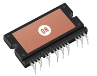
Intelligent Power Module
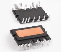
The FPAB20BH60B is an advanced PFC SPM 3 module providing a fully-featured, high-performance Boost PFC (Power Factor Correction) input power stage for consumer, medical, and industrial applications. These modules integrate optimized gate drive of the built-in IGBT to minimize EMI and losses, while also providing multiple on-module protection features including under-voltage lockout, over-current shutdown, thermal monitoring, and fault reporting. These modules also feature a full-wave rectifier and high-performance output diode for additional space savings and mounting convenience.
|
|
|
The NXV65HR51DZ is an OnBoard Charger H-Bridge in the APM16 Series for LLC and Phase-shifted DC-DC Converters. It is a 51mOhm SuperFET3 H-Bridge on Al²O³ DBC substrate with 5kV isolation in a compact APM16 transfer molded module.
|
|
|
Isolated Gate Driver
NCD57000DWR2G Isolated High Current IGBT Driver, High Side and Low Side, 7.1A, 3.3V to 5V Supply, 60ns/66ns Delay, WSOIC-16
The NCD57000 is a high−current single channel IGBT driver with internal galvanic isolation, designed for high system efficiency and reliability in high power applications. Its features include complementary inputs, open drain FAULT and Ready outputs, active Miller clamp, accurate UVLOs, DESAT protection, soft turn−off at DESAT, and separate high and low (OUTH and OUTL) driver outputs for system design convenience. The NCD57000 accommodates both 5 V and 3.3 V signals on the input side and wide bias voltage range on the driver side, including negative voltage capability. The NCD57000 provides > 5 kVrms (UL1577 rating) galvanic isolation and > 1200 Viorm (working voltage) capabilities. The NCD57000 is available in the wide−body SOIC−16 package with a guaranteed 8 mm creepage distance between input and output to fulfill reinforced safety insulation requirements.
|
|
|
Non isolated gate driver
The FAN3223 to -25 family of dual 4A gate drivers is designed to drive N-channel enhancement-mode MOSFETs in low-side switching applications by providing high peak current pulses during the short switching intervals. The driver is available with either TTL or CMOS input thresholds. Internal circuitry provides an under-voltage lockout function by holding the output LOW until the supply voltage is within the operating range. In addition, the drivers feature matched internal propagation delays between A and B channels for applications requiring dual gate drives with critical timing, such as synchronous rectifiers. This also enables connecting two drivers in parallel to effectively double the current capability driving a single MOSFET. The FAN322X drivers incorporate MillerDrive architecture for the final output stage. This bipolar-MOSFET combination provides high current during the Miller plateau stage of the MOSFET turn-on / turn-off process to minimize switching loss, while providing rail-to-rail voltage swing and reverse current capability. The FAN3223 offers two inverting drivers and the FAN3224 offers two non-inverting drivers. Each device has dual independent enable pins that default to ON if not connected. In the FAN3225, each channel has dual inputs of opposite polarity, which allows configuration as non-inverting or inverting with an optional enable function using the second input. If one or both inputs are left unconnected, internal resistors bias the inputs such that the output is pulled LOW to hold the power MOSFET OFF.
|
|
MillerDrive Technology
|
Opto Gate Driver
The FOD3120 is a 2.5A output current gate drive optocoupler, capable of driving most 800V/20A IGBTs/MOSFETs. It is suited for fast switching driving of power IGBTs and MOSFETs used in motor control inverter applications, and high performance power systems. It utilizes ON Semiconductor’s proprietary coplanar packaging technology, Optoplanar, and optimized IC design to achieve high noise immunity, characterized by high common mode rejection. It consists of a gallium aluminum arsenide (AlGaAs) light emitting diode (LED) optically coupled to an integrated circuit with a high-speed driver for push-pull MOSFET output stage.
|
|
100ns max. pulse width distortion
|
Power Switchers
The SUPERFET III MOSFET is ON Semiconductor’s brand−new high voltage super−junction (SJ) MOSFET family that is utilizing charge balance technology for outstanding low on−resistance and lower gate charge performance. This advanced technology is tailored to minimize conduction losses, provide superior switching performance, and withstand extreme dv/dt rates. The SUPERFET III MOSFET Easy drive series helps manage EMI issues and allows for easier design implementation.
|
|
Internal Gate Resistance: 1 Ω
|
Giveaway: Register here to win ON Semiconductor’s NCP51705SMDGEVB silicon carbide evaluation board designed on a four-layer printed circuit board which includes the NCP51705 driver and all the necessary drive circuitry.
For more information: about On Semiconductor's power management products, click here for more information.
Test Your KnowledgeBack to Top

Are you ready to demonstrate your knowledge of High Power Conversion and Wide Bandgap Technology? Then take a quick 5-question quiz to see how much you've learned. To earn the DC Power III Badge, read through the learning module, attain 100% on the quiz, leave us some feedback in the comments section, and give the learning module a star rating.
| DCPower3.pdf |

Top Comments