


Designers of power adapters face the challenge of delivering more power in smaller packages while maintaining high efficiency. The adoption of Gallium Nitride (GaN) technology mitigates this problem by enabling unprecedented power density and efficiency improvements over traditional silicon-based solutions. GaN's wide bandgap properties allow higher switching frequencies, lower losses, and superior thermal performance. These are the key factors that drive the miniaturization of power conversion systems.
This technical overview shows how GaN technology transforms power adapter design through better power density and efficiency. We'll explore the path to higher power density, analyze GaN's role in achieving higher density, and see how these features enable compact, high-performance power solutions - principles demonstrated in CUI Inc.'s SDI200G-U Series, which showcases GaN's capabilities in power adapters. Related Components | Test Your Knowledge
2. Understanding Power Density
Power density is the measure of power output per unit volume. It is expressed in watts per cubic inch (W/in³) or watts per cubic centimeter (W/cm³). Mathematically, power density (Pd) can be expressed as:
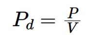
where P is power (W) and V is volume (in³ or cm³).
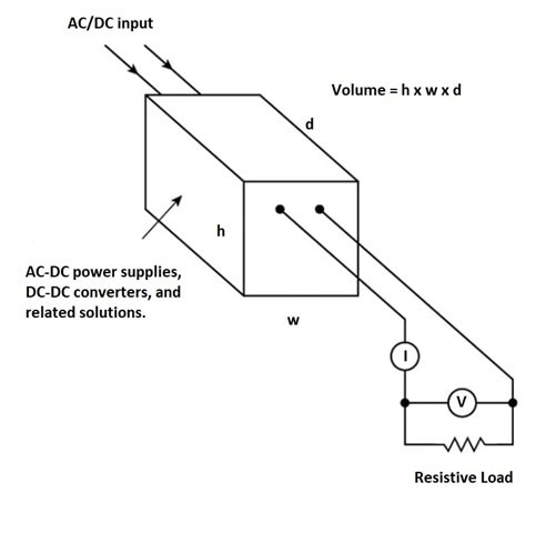
Figure 1: The figure visualizes the concept of power density. (image source: element14)
For example, a 200W power adapter in a 4.3 in³ enclosure achieves a power density = 200W / 4.3 in³ = 46.5 W/in³.
3. The Path to Higher Power Density
What is the main barrier to achieving higher power density in power management systems? Three fundamental challenges must be overcome while maximizing power density in modern power systems: switching losses, thermal constraints, and space limitations. A strategic approach that combines advanced semiconductor technology, optimized circuit design, and robust thermal management is required to address these effectively.
- Leverage Advanced Semiconductor Materials: GaN has high electron mobility, lower RDS on (drain-source on-resistance), compared to traditional silicon that helps enable greater efficiency.
- Optimize Thermal Management: Ideal heat management should be like fluid dynamics that establish clear, efficient pathways ensuring heat is rapidly transferred away from critical components. enhanced packaging and advanced lead frame technologies minimizes thermal resistance and improves heat dissipation. A shorter thermal path leads to better thermal efficiency, improved reliability, and higher power density.
- Higher Switching Frequencies: Higher switching frequencies allow for smaller passive components (inductors and capacitors), reducing overall system size. However, simply increasing frequency isn't enough—soft-switching techniques (such as zero-voltage or zero-current switching) must be employed to minimize stress on components and maintain efficiency.
- Enhance Integration for a Smaller Footprint: Modern designs integrate power and control elements monolithically or through multichip module (MCM) technology, combining multiple semiconductors, dies and even passive components within a single package. This approach drastically reduces the overall system footprint while maintaining performance and reliability.
4. Relationship between Efficiency and Power Density
Power density and efficiency are closely connected factors in modern power converter design. Power density measures the output power per unit volume, while efficiency shows how effectively input power converts to usable output. Higher efficiency reduces heat generation, allowing for more compact designs and improving power density.
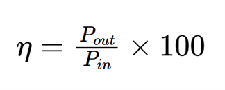
Where η is efficiency.
Pout is output power, and Pin is input power.
The relation can be understood by the following technical aspects:
- Thermal Management: High power density systems generate significant heat due to the concentration of power in a small volume. This results in reduced power efficiency. Therefore, this heat must be dissipated efficiently to maintain system reliability and performance. The relationship can be expressed as
Ploss = Pin − Pout
Where Ploss represents power losses, primarily due to resistive losses, switching losses, and thermal dissipation, High power density exacerbates Ploss, thereby reducing efficiency. - Component Sizing and Materials Property: Miniaturizing components is a step towards achieving high power density. However, smaller components tend to be of reduced efficiency as they have higher parasitic resistances and lower thermal capacities, leading to increased losses. This can be understood using the formula:
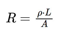
R = Resistance (Ω)
ρ = Resistivity of the material (Ω·m)
L = Length of the conductor (m)
A = Cross-sectional area (m²)Reducing A to increase power density increases R, which leads to higher power losses and lower efficiency.
- Switching frequency: In power electronics, increasing the switching frequency of converters (e.g., DC-DC converters) can reduce the size of passive components, thereby increasing power density. However, higher switching frequencies result in higher switching losses, which can be approximated as:
Psw = Switching losses (W)
V = Voltage across the switch (V)
I = Current through the switch (A)
trise and tfall = Rise and fall time of the switch (s)
fsw = Switching frequency (Hz)These losses reduce overall efficiency, highlighting the trade-off between power density and efficiency.
5. Understanding Gallium Nitride (GaN)
Gallium Nitride (GaN) is a wide-bandgap semiconductor with a bandgap of 3.4 eV (compared to silicon’s 1.1 eV). It is a binary III/V direct bandgap semiconductor with a robust Wurtzite crystal structure, making it highly stable and efficient for high-power applications. Unlike silicon, GaN substrates do not occur naturally and must be synthetically produced. A thin aluminium gallium nitride (AlGaN) layer is grown on top of the GaN crystal, creating strain at the interface to enhance its conductivity. This strain induces a two-dimensional electron gas (2DEG), which allows for highly efficient electron conduction when an electric field is applied.

Figure 2: The basic configuration of GaN HEMT (Image source)
6. Enabling High Power Density and Efficient Systems with GaN
Higher breakdown voltage, lower conduction losses, and faster switching speeds of GaN power devices enable them to outperform traditional silicon-based devices. These devices can switch at higher frequencies (MHz range) while maintaining low on-resistance and minimal switching losses. This allows power supplies to achieve smaller form factors and higher efficiencies, crucial for compact desktop adapters. This allows power supplies to achieve smaller form factors and higher efficiencies, crucial for compact desktop adapters. GaN increases power density through several mechanisms:
- Higher switching frequencies: GaN transistors switch much faster than silicon MOSFETs, often operating at MHz frequencies instead of the typical 100–500 kHz. They have low gate charge (Qg) and reduced output capacitance (Coss), which allow rapid turn-on and turn-off times. Some GaN devices achieve switching speeds exceeding 200 V/ns, minimizing transition losses. Additionally, GaN’s high electron mobility (~2000 cm²/V·s) further enhances switching speed, while its low gate charge and reduced capacitances help minimize energy losses.
- Reduced conduction and switching losses: GaN devices have lower on-resistance (RDS(on)), which reduces conduction losses and improves efficiency. Unlike silicon MOSFETs, GaN transistors do not have a body diode, eliminating reverse recovery losses in hard-switching applications.
- Figure 3 illustrates the theoretical limits of silicon, GaN, and silicon carbide (SiC), showing that for a given breakdown voltage, WBG (wide band gap) materials have significantly lower RDS(on) than silicon—with GaN being the lowest.

Figure 3: Theoretical Limits of RDS(on) or Ronvs. breakdown voltage for Si, GaN, and SiC transistors (Image source)
- Better Thermal Performance: Although GaN’s thermal conductivity (~1.3 W/mK) is slightly lower than silicon (~1.5 W/mK), its superior efficiency reduces overall heat generation. This means power systems can run cooler even at higher power densities, reducing the need for bulky heat sinks and fans. GaN devices can also tolerate higher operating temperatures (up to 150°C vs. 125°C for silicon) without compromise in performance. This makes them ideal for high-temperature environments, such as industrial and automotive applications.
- High voltage handling and reliability: Most GaN transistors operate at voltages up to 650 V, making them suitable for applications like DC-DC converters, motor drives, and power supplies. High-voltage GaN (>1 kV) solutions are expanding their use in industrial and grid applications. Additionally, GaN’s high electron mobility (~2000 cm²/V·s) enhances switching performance and reduces energy losses.
- Advanced integration for higher power density: GaN technology allows power transistors, gate drivers, and logic circuits to be combined in a single chip. Such monolithic integration reduces parasitic inductance, enhances switching performance, and simplifies circuit design. New GaN System-in-Package (SiP) and System-on-Chip (SoC) solutions integrate multiple functions, minimizing external components and further boost ng power density. These highly compact designs are transforming next-generation power modules, automotive inverters, and fast-charging systems.
7. Designing High Power Density Chargers and Adapters with GaN
Selecting the right topology is key to maximizing GaN's efficiency, power density, and thermal performance in high-performance chargers and adaptors. GaN High Electron Mobility Transistors (HEMTs) enable higher switching frequencies, reducing passive component size while maintaining efficiency.
- Quasi-Resonant (QR) Flyback: The QR flyback topology is widely used in charger/adapter designs because it is simple, cost-effective, and offers easy control with good transient response. It uses valley-switching to cut down turn-on losses, though some losses persist, especially at high input voltage (above 220 VAC). QR flyback excels in light-load efficiency, a key requirement for chargers/adapters. However, it only works in discontinuous conduction mode (DCM), and transformer leakage energy is managed with an RCD snubber. This results in higher peak and RMS currents compared to resonant converters, which have smoother, sinusoidal currents. QR flyback operates at variable frequencies, which complicates MI filter design. A more advanced version, the ZVS QR flyback, ensures lossless turn-on for the primary switch, boosting efficiency, particularly at high input voltages. This topology can achieve frequencies up to 300 kHz, delivering higher efficiency and power density.
- Active-Clamp Flyback (ACF): This is a leading flyback topology that enables Zero Voltage Switching (ZVS) for FETs, making it ideal for high-frequency operation. Unlike QR Flyback, ACF recovers transformer leakage energy instead of dissipating it and improves EMI by clamping the primary FET voltage with a capacitor. ACF operates in two modes: Complementary Mode (CP), where the main and clamp switches alternate each cycle, achieving ZVS but increasing switching frequency at light loads, impacting efficiency and EMI. Non-Complementary Mode (NCP) activates the clamp switch only as needed to store energy for ZVS, minimizing circulating currents and conduction losses. NCP ACF is the preferred choice for better light-load efficiency and lower losses.
- Hybrid Flyback (HFB): : Hybrid Flyback (HFB) combines Zero Voltage Switching (ZVS) and Zero Current Switching (ZCS) for high efficiency at high frequencies. Its use resonant waveforms to lower RMS currents and reduce transformer size. The resonant capacitor aids energy storage, cutting overall transformer requirements. The half-bridge structure with a HFB self-clamping mechanism enables it to outperform Active Clamp Flyback (ACF) in voltage stress handling. However, the presence of circulating currents demands careful light-load efficiency management as it adds an extra FET on the primary side. Universal input compatibility also requires precise design considerations.
8. SDI200G-U series from CUI Inc: Pushing Power Density Boundaries with GaN Technology
The SDI200G series represents a significant transformation in power supply technology by using GaN Systems' transistors instead of traditional silicon-based components. This desktop AC-DC power supply delivers 192–200 W output power with voltage options ranging from 12 V to 56 V DC.The series achieves an impressive 216% increase in power density (from 5.3 W/in³ to 11.4 W/in³) compared to its silicon counterpart, while reducing weight by 32%—from 820 g to 560 g. It delivers 96% efficiency while operating across an input voltage range of 90–264 VAC.The SDI200G-U series has also exceeded DoE Level VI and EU 2019/1782 standards, with a remarkably low no-load power consumption of just 0.21 W.
The compact design measures only 161 x 54.2 x 33.2mm and incorporates comprehensive protection features including OCP, OTP, OVP, and short circuit protection. The SDI200G-U series comes with UL/cUL 62368-1 certification and multiple safety approvals (CE, FCC, UKCA), features power factor correction (PFC) and is well-suited for ICT and AV applications where compact size, efficiency, and portability are key considerations.
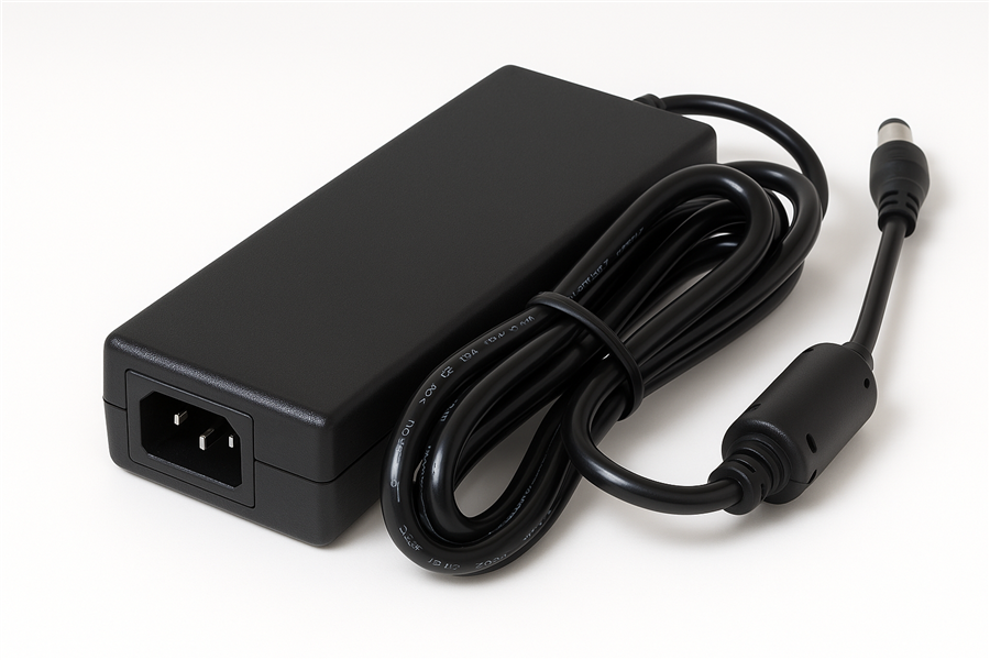
Figure 4: SDI200G-U Series Three Prong (C14) Ac-Dc Desktop Adapter(Image source)
9. Conclusion
GaN power adapters deliver significant advantages over traditional silicon-based designs. It's wide bandgap properties enable higher switching frequencies, reducing internal component size and allowing for a smaller, lighter form factor ideal for portable applications. The lower on-state resistance and minimal conduction losses make GaN more efficient, while reduced gate and output charges further improve performance. Additionally, it’s superior thermal conductivity supports higher operating temperatures and efficient heat dissipation, ensuring reliable and cooler operation. These advantages make GaN the ideal choice for high-performance power adapters.
10. Frequently Asked Questions on GaN Technology and Power Density
What is maximum power density?
Maximum power density refers to the highest amount of power that can be delivered per unit volume in a power system. It depends on several factors, including the efficiency of power conversion, thermal management, and the materials used.
What does GaN HEMT stand for?
GaN HEMT stands for Gallium Nitride High Electron Mobility Transistor. It is a type of field-effect transistor (FET) that leverages the superior electron mobility of GaN to enable high-speed switching, low resistance, and improved efficiency in power electronics.
What is the best power density?
The best power density depends on the application. Achieving high power density requires balancing efficiency, thermal management, and circuit design.
What is the standard power density?
There is no single "standard" power density, as it varies by application.
Is high power density good?
Yes, high power density is beneficial as it allows for smaller, lighter, and more efficient power converters. It is especially useful in applications like consumer electronics, data centers, and automotive systems. However, it requires effective thermal management to prevent overheating.
What is the disadvantage of GaN?
The primary disadvantages of GaN include higher cost, manufacturing complexity, and challenges arising from thermal management issues. Due to advanced manufacturing processes, GaN devices are more expensive than their silicon counterparts. Although more efficient, they can generate concentrated heat, requiring careful heat dissipation. Furthermore, integrating GaN into existing designs requires specialized packaging and expertise.
Which semiconductor material is better than Gallium Nitride?
Currently, Silicon Carbide (SiC) is a strong competitor to GaN, especially in high-power applications above 600V, such as electric vehicles and industrial power systems. SiC offers excellent thermal conductivity and voltage handling but lacks GaN’s high-speed switching advantages at lower voltages.
Is GaN replacing silicon?
GaN is gradually replacing silicon in high-frequency, high-efficiency power applications, particularly in chargers, adapters, and RF power amplifiers. However, silicon remains dominant in lower-cost, lower-frequency applications due to its well-established manufacturing ecosystem.
What are the cons of GaN chargers?
GaN chargers have a few drawbacks, including:
- Higher Cost – More expensive than traditional silicon-based chargers.
- Thermal Hotspots – Despite high efficiency, GaN can generate concentrated heat, requiring improved cooling solutions.
- Limited High-Voltage Applications – While excellent at low to mid-range voltages, GaN is less common in ultra-high-voltage applications compared to SiC.
What is the smallest GaN power supply?
The smallest GaN power supplies are ultra-compact USB-C chargers.
Why can GaN switch faster?
GaN can switch faster because it has higher electron mobility and lower gate charge compared to silicon. This allows it to turn on and off at higher frequencies with minimal energy loss, reducing switching losses and enabling more efficient, compact power converters.
*Trademark. CUI is a trademark of CUI Corporation. Other logos, product and/or company names may be trademarks of their respective owners.


For more CUI products Shop Now
Test Your Knowledge
GaN Power Density

Are you ready to demonstrate your knowledge about this topic? Then take a quick 10-question multiple choice quiz to see how much you've learned from this module.
To earn the Essentials of GaN Power Density Badge, read through the learning module and attain 100% in the quiz.


-

rscasny
-
Cancel
-
Vote Up
0
Vote Down
-
-
Sign in to reply
-
More
-
Cancel
Comment-

rscasny
-
Cancel
-
Vote Up
0
Vote Down
-
-
Sign in to reply
-
More
-
Cancel
Children