

 Billions of images get uploaded daily. It's now a cliché to freeze a moment in time, capture life by digital means, and cherish the memory for years to come. Have you ever paused to think of how a camera detects an image and processes it in digital form or how images become clear and sharp in varied lighting conditions? Camera performance (read: superior image quality) is crucial for some use-cases like automotive and artificial intelligence. This blog explains the technology inside the camera and how its sensing element (image sensor) works.
Before we begin, it is necessary to understand a few image processing terms:
Image Sensors
Shop our wide variety of images sensors for use in gaming systems, surveillance, HD video, Machine Vision, motion monitoring, and barcode scanning.
- Image sensor: An essential sensing element of any camera that captures light and converts it into an electrical signal. This signal is transmitted to an imaging device processor to produce a digital image. A Bayer filter is used in the color image sensor to create a raw image.
- Raw image: This is an uncompressed image file. It is called a Raw image as it is minimally processed data collected from the camera's image sensor while sourcing all relevant information for image processing.
- YUV image: YUV is a color encoding system or a representation of color where "Y" indicates luminance (brightness), "U" and "V" means chrominance (color). This RGB representation reduces the file size since 3 bytes are used in RGB to store color, and YUV uses only half the size.
- Image signal processing pipeline: This is a process to convert an image into digital form using functions like noise reduction, demosaicing, autofocus, auto exposure, auto white balance, and image sharpening designed for digital processing and image quality enhancement.
- Auto-exposure (AE) and auto-white balance (AWB): These detects the continually changing ambient light qualities of the scene and adjusts the camera to maintain the right brightness and color.
With the opening of the camera shutter, light (photons) passes through a lens (imaging optics) and color filter array, and finally, hit the image sensors (photodiodes). The photons are converted into an electrical signal again, amplified and reconverted into digital form using an ADC. After exposure, the photons that reach each photosite generate an electrical signal, varying in strength depending on the photons captured inside the cavity. The information is sewn together to obtain a Raw image. Figure 1 shows an imaging system pipeline from capturing the scene to image enhancement and compression.

Figure 1: Imaging System Pipeline ( Image Source: IEEE Circuits and Devices )
Image Sensor Architecture
An image sensor is made up of an array of pixels, and each pixel contains a photodetector that converts incident light into photocurrent. It includes some of the readout circuits needed to convert the photocurrent into voltage and to read it off the array, as shown in figure 2. The percentage of area occupied by the photodetector in a pixel is known as the fill factor. The rest of the readout circuits are located at the array's periphery and multiplexed by the pixels. Pixel circuits are mainly divided into active pixels (APS) and passive pixels (PPS). APS are sensors that implement a buffer per pixel simply as a source-follower. Passive pixels (PPS) are based on photodiodes without internal amplification.


Figure 2: Internal architecture of image sensor and APS schematic ( Image Source: Microelectronics Journal )
Image Sensor Types
Image sensors are fabricated using metal-oxide-semiconductor technology and can be categorized into two types as per their pixel element: Charged Couple Device (CCD) and CMOS sensor (aka active pixel sensor). CCD is based on the MOS capacitor, whereas CMOS is based on the MOSFET amplifier.
Complementary Metal Oxide Semiconductor (CMOS) Sensor
A CMOS image sensor has a photodiode and a CMOS transistor switch for each pixel in the pixel array and permits individual amplification of the pixel signals. A matrix of switches enables the pixel signals to be sequentially and directly accessed. Most modern sensors are of CMOS variety. A microlens implemented over the Bayer filter helps each pixel capture the maximum quantum of light. The pixels are not precisely mutually positioned as a tiny gap exists between them. Any light which falls into such a gap is wasted light and will not be used for exposure. These microlenses want to erase this light waste by directing the light, which falls between the two pixels.
Figure 3: CMOS Image Sensor CMOS Image Sensor
Charge-Coupled Device (CCD)
When light hits the chip In the CCD image sensor, it transforms into a small electrical charge and is stored in each photosensor. The charges present in the pixel line closest to the output amplifiers get amplified and reworked to an output, followed by the individual line of pixels shifting their charges one line nearer to the amplifier. The process is subsequently repeated by moving the charge until all the pixels lines changed into an output. An analog-to-digital converter (ADC) subsequently turns an individual pixel's value into a digital form by quantifying the volume of charge at each photosite and then turning that measurement into its binary form.
Getting Colored Image by Bayer Transformation
The Bayer filter that produced a colored image is an integrated camera part. The color gets filtered at each photosite and traps alternating red, green, and blue color photosites so that green photosites get recorded twice concerning the other two colors. The filter pattern is thus 50 percent green, 25 percent red, and 25 percent blue. It is then represented as BGGR, RGBG, GRGB, or RGGB. This happens as the human eye is more prone to green color. The values from such photosites are then judiciously combined to generate full-color pixels using the "demosaicing" process. These values are further processed via an image signal processing pipeline technique to achieve superior quality. A color photosites' Bayer filter pattern side view is shown in Figure 4.

Figure 4: Bayer Filter pattern and color photosites ( Image Source: PathPartnerTech )
Image Signal Processing
The RAW image from the image sensor needs significant processing to be converted into a high-quality image. Image signal processing (ISP) is used in such instances. An ISP is a dedicated processor that converts the camera sensor-generated raw data into a functioning image format. Figure 5 shows an image signal processing pipeline with distinct processing stages, which play a crucial role in making a premium quality image. The ISP fulfills many of the following steps to supply a high-quality image for a specific camera sensor and use-case:

Figure 5: image signal processing pipeline ( Image Source: IEEE Signal Processing )
1. Preprocessing: The sensor generated raw data must be processed before full-color image production to eliminate noise (among other artifacts) beside a color processing pipeline to generate an accurate or a photogenic representation of that captured scene. A standard preprocessing procedure is defective pixel correction. Certain sensor photo-elements can be defective and, if uncorrected, crops up as confetti-like errors post demosaicing. The estimation of such missing or defective pixels is done by interpolating the accurately recorded data in their neighborhood. In some cases, preprocessing also includes linearization, dark current compensation, and flare compensation.
2. White Balancing: White balance (WB) is a process to remove unrealistic color casts so that white objects in real life are rendered white in an image. Human eyes are excellent at judging white color under different light sources. Still, digital cameras develop complications with auto white balance (AWB) and may create displeasing blue, orange, or sometimes green color casts. Correct camera white balance must include the "color temperature" of that particular light source, citing the relative coolness or warmth of white light. The white balance, other than color temperature, employs another technique termed green-magenta shift. It is unnecessary to adjust the green-magenta shift under ordinary daylight. Artificial lighting (like fluorescent lighting) may need considerable green-magenta adjustments to WB.
3. Demosaicing: Demosaicing is an image processing algorithm used to reconstruct full-resolution color images from sampled data acquired from an image sensor that uses a color filter array (CFA). It is also known as CFA interpolation or color reconstruction. Demosaicing methods are divided into three groups. Heuristic approaches comprise the first group. The second group expresses demosaicing as a restoration complication. The third group constitutes a generalization which employs a spectral filtering model. The demosaicing techniques are usually either proprietary or under patents. All demosaicing methods utilize pixel neighborhood information to estimate non-measured pixel colors' values.
4. Color Transformation: Color transformation (aka color space conversion) is the translation of color representation from a basis to another. It generally happens in converting an image represented in one color space to yet another color space. The aim is to make that translated image appear identical (or closest to it) to the original. Color space denotes a particular color organization that permits reproducible analog and digital representations of color. A color space can be arbitrary, with specific colors assigned to physical color swatches set and analogous assigned color numbers or names (the Pantone collection), or be structured mathematically (the NCS System,sRGB, and Adobe RGB).
5. Postprocessing: Postprocessing is a requisite as every individual previous step may inject objectionable artifacts. A good example is a demosaicing step inserting a zipper artifact beside strong intensity edges. The common postprocessing steps include removal, coring, and edge enhancement. These methods are mostly heuristic-based and need to be substantially fine-tuned. The human eye is highly sensitive to sharp edges, noticeably to the vertical and horizontal edges compared to diagonal ones, and even numb to edges in the other directions. The majority of camera manufacturers use an edge-enhancement step, such as unsharp masking, to enhance image appeal by reducing the image's low-frequency content in the image. Coring removes insignificant image detail information.
6. Display, Compress, and Store: Image data must be remolded into the appropriate color space dependent on reproduction media like printer type or computer monitor. A CRT monitor is a good example in this context. In this case, the data must be changed into an 8-b format, anticipating the display model (gamma values, color temperature, and offsets). When it comes to dye-sublimation printer (four-color, subtractive color), the data is changed into a CMYK color space using the correct color reproduction model.
Current implementations store the images in either a proprietary file format or a recently developed tagged image file format for electronic photography (TIFF/EP). The TIFF/EP files are standard TIFF files, but supplementary file tags store linearization function, camera settings details, spectral sensitivities, color transform matrix, and illuminant used information. The image data is generally stored in a mosaicked form. Consumer cameras mostly use EXIF format, as it is compact and easy to implement in hardware. Another alternative is the baseline JPEG algorithm.
Image Sensor Module and Selection Criteria
An image sensor module includes lens assembly, photodetectors, amplifiers, and sensors on a single PCB and connected to an external SoC for further image processing. These modules can integrate multiple attributes on a single silicon die since the pixel array includes autofocus (AF) drivers, lens shading correction (LSC) algorithms, and also innovative solutions, like high dynamic range (HDR) technology with substantial system on chip (SoC) prowess.
There are different kinds of image sensor modules. The two most common ones are the Raw Image Sensor Module and the YUV Image Sensor Module.
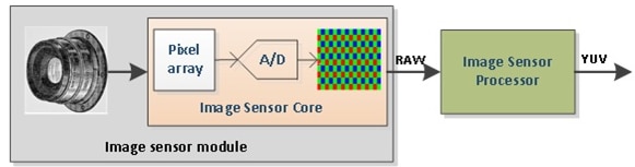
Figure 6: Image sensor module ( Image Source: einfochips.com )
Raw image sensor modules offer raw image output of uncompressed and unprocessed data. An external ISP processor is thus required for further image processing to produce a quality image. In contrast, the YUV image sensor module packs an inbuilt ISP pipeline and gives YUV image data as output. Since the image pipeline is hardware-implemented, completion of front-end image processing does not impose any processing burden on the main application processor. In such cases, the Host SoC has no ISP requirement, and data is directly compressed, stored in memory, or streamed out conditional on application.
Image sensor selection is a specification based such as:
- Horizontal Pixels: The pixel population in an image sensor row
- Maximum Frame Rate: Number of frames every second.
- Pixel Size: Biggest pixel dimension
- Data Rate: The data transfer process speed, generally expressed in bytes per second or bits per second
- Supply Voltage: The supply voltage range for the image sensor
- Maximum Power Dissipation: The power lost due to the image sensor's thermal dissipation
- Dynamic Range: The logarithmic ratio of good depth to readout noise in decibels. A higher number equals a better dynamic range.
- Image Sensor Output: The digital output of the sensor, such as 8 bit, 10 bit, 12, bit, 16 bit, etc.
- Quantum Efficiency: Ratio of photon-generated electrons captured by the pixel to the photons hitting the pixel area.
- Vertical Pixels: Pixel population in an image sensor column. The greater the number of pixels makes the better resolution.
The other criteria include Sensitivity in Lux/s, Resolution in dpi, and Support for a wide variety of spectrums.
Top Comments