Introduction
Semiconductors are essential components used in nearly all electronic circuits today, and include devices such as diodes, transistors, and integrated circuits. By definition, semiconductors have an electrical conductivity between a conductor and an insulator. Silicon happens to be the most abundant material for use in semiconductors, and up until now has been the favored semiconductor material. As the technology evolves towards towards smaller, more robust, and handier devices, the theoretical constraints on existing semiconductor materials may have been reached. Thus, other semiconductor materials are being considered as substitutes for silicon. Gallium Nitride is one of those substitutes. In this article, we will spotlight Gallium Nitride (GaN), a distinctive semiconductor material which may be capable of surpassing silicon semiconductors in an expansive list of applications. A comparative study of Silicon and Gallium Nitride material properties, applications, and uses will be discussed and help you to understand the opportunities created by GaN semiconductor materials in recent years.
What is Gallium Nitride?
Gallium nitride (GaN), is a binary III/V direct bandgap semiconductor having a robust Wurtzite crystal structure. GaN substrates are not naturally occurring compounds. It is a semiconductor material produced in the laboratory by combining one atom of gallium with one atom of nitrogen. It is usually riddled with multiple crystal defects over a small area, at times reaching millions of defects per centimeter range. However, new manufacturing techniques like metal-organic chemical vapor deposition (MOCVD) have diminished the number of defects to anywhere from 100 to 1000 per centimeter, allowing GaN to have greater potential in semiconductor applications.
GaN Semiconductors
Shop our wide variety of GaN Semiconductors, including transistors, converters, LED drivers, and development boards.
Characteristics of Gallium Nitride and Silicon Semiconductors
The electrical and chemical properties of both Silicon and Gallium Nitride semiconductors should be understood to use them. The GaN semiconductor material promises better attributes over legacy Silicon material in certain areas:
- The Bandgap of Semiconductors: The energy bandgap (which relates to how well a material conducts electricity) of Gallium nitride is 3.4 eV, compared to Silicon’s 1.12 eV. GaN’s wide-bandgap characteristic allows devices to sustain much higher voltages and temperatures. This feature simultaneously restricts GaN's usage in diminished voltage applications.
- Breakdown Field: GaN's breakdown field is 3.3 MV/cm, while silicon has a breakdown field of 0.3 MV/cm. A higher breakdown field allows GaN devices to operate at higher voltages and lower leakage currents.
- Electron Mobility: Silicon has an electron mobility of 1500 cm2/Vs, while Gallium nitride has an electron mobility of 2000 cm2/Vs. The Gallium nitride crystals’ electrons can move 30% faster than silicon's electrons. This electron mobility offers GaN an undeniable advantage in higher switching frequencies.
- Operating Temperature: A silicon device’s typical operational maximum temperature is roughly 150°C. GaN semiconductors can operate at higher temperatures, up to 400°C, with high mobility. These combined characteristics make GaN highly desirable in high temperature, high frequency, and high power environments. Nevertheless, no product is released today with this feature.
- Thermal Conductivity: Thermal conductivity measures a material’s ability to conduct heat. Gallium nitride has a thermal conductivity of 1.3 W/cmK, while silicon has a thermal conductivity of 1.5 W/cmK. GaN’s relatively poor thermal conductivity makes heat management a challenge for system designers.
GAN vs Silicon Transistors
Transistors revolutionized the electronics industry, and silicon-based transistor devices have thrived across multiple domains. However, silicon transistors at high voltages reveal lackluster performance, due to weak electric strength, specifically in power MOSFET applications.
GaN transistors have significant advantages over silicon MOSFETs in terms of switching speed and power conversion efficiency. GaN is a high electron mobility transistor (HEMT), as shown in Figure 1. The high electron mobility means that a GaN transistor will have a smaller size for a given on-resistance and breakdown voltage than a silicon transistor. GaN transistors can operate at higher temperatures and higher current densities than their Si counterparts. Such properties make GaN transistors well-suited for high power, high frequency and wide bandwidth applications in extreme environments, as listed in the application section. Since the individual transistors are smaller than their silicon counterparts, many more GaN transistors can be produced per wafer, thus forming a situation where GaN devices may have a competitive manufacturing advantage vis-à-vis their silicon cousins.
Figure 1. GaN HEMT Structure
Like a Silicon MOSFET, a GaN FET has a source, drain, and gate. GaN FETs operate speedily, with lower gate threshold voltages, and need customized gate drivers to satisfy requirements. The GaN FET’s internal-gate resistance is much lower and there is no reverse recovery charge, unlike silicon FETs. A Barrier semiconductor layer isolates the gate and the channel so that minimal current flows between the channel and the gate. In GaN FETs, the barrier is typically made of aluminum gallium nitride (AlGaN) or Indium aluminum nitride (InAlN).
The substrate is the last and thickest layer of the vertical structure. It provides mechanical support, heat spreading, and electromagnetic confinement. GaN FETs use a foreign substrate to avoid costly issues. The following list names a few widely used substrates:
- GaN-on-silicon carbide or GaN-on-SiC
- GaN-on-silicon or GaN-on-Si
- GaN-on-sapphire
- GaN-on-insulator
- GaN-on-hexagonal boron nitride or GaN-on-h-BN
- GaN-on-diamond
Different substrates have different advantages, and also suffer different levels of mismatch. GaN on Silicon is a relatively inexpensive substrate compared with silicon carbide (SiC). The GaN-on-SiC structure has a high thermal conductivity, which allows GaN MOSFETs to dissipate more power without increasing the device temperature. GaN and SiC are lattice-matched, creating a lower defect density of the crystals, reducing leakage and improving reliability. For GaN to grow on Si, a more complicated epitaxial (epi) structure is required to keep the wafer from warping, and impacting the time, cost, and performance of the semiconductor.
Applications
The high abundance, moderate bandgap, and easy fabrication characteristics of silicon semiconductors enabled them to permeate every facet of the electronics industry, from solid-state devices in computers, solar cells, MEMS, power devices, mixed-signal circuits, RF electronics, and more. GaN materials already dominate the optoelectronics industry in LEDs, lasers, and Blu-ray players, and they have significantly impacted diverse industries over the past decade. Technological advancements enable GaN's properties to be used for fast, high-power, high-efficiency, and high-temperature electronics applications such as he following:
- High radio frequency components, such as RF power amplifiers and 5G telecommunication up to 100 GHz
- Wireless power transmission, such as wireless chargers for phones, laptops, game console controllers, heart pumps, and other medical applications
- Switch−mode power supply applications, such as DC−DC converters and inverters up to 1000 V
- Solar cells for photovoltaic systems
- Small, fast-charging power adapters and motor drives for appliances
- LiDar (light detection and ranging) devices in autonomous cars that measure distances using lasers
- Imaging and sensing applications like power amplifiers for microwave and terahertz (THz) devices

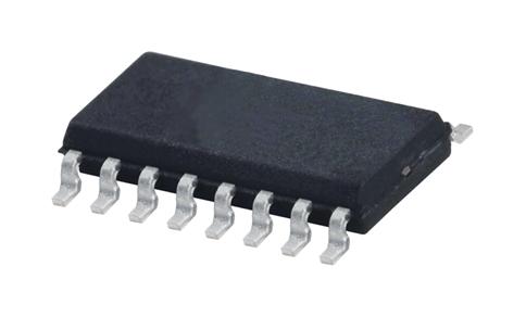
Figure 2: Infineon GaN EiceDRIVER gate driver ICInfineon GaN EiceDRIVER
gate driver IC
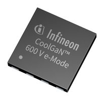
GaN-centric products are increasingly being designed and fabricated today. As an example, Infineon’s 1EDS5663HXUMA1 is a high side gate driver IC which acts as an intermediate between a control IC and power FETs. With excellent robustness and efficiency, the single-channel galvanically isolated driver IC is a perfect fit for enhancement mode (e-mode) GaN HEMTs with a non-isolated gate and low threshold voltage. The driver IC has a fast input-to-output propagation (37 ns) with excellent stability. It is used for robust operation in hard-switching DC-DC applications and meets safe isolation demand. Infineon CoolGaN and similar GaN switches require a continuous gate current of a few mA in their "on" state. Besides, due to low threshold voltage and extremely fast switching transients, a negative "off" voltage level may be needed. The widely used RC-coupled gate driver fulfils these requirements, however it suffers from a duty-cycle dependence of switching dynamics and the lack of negative gate drive in specific situations. Infineon's GaN EiceDRIVER
solves these issues with very low effort. The two output stages shown below enable a zero “off" level to eliminate any duty-cycle dependence. In addition, the differential topology is able to provide negative gate drive without the need for a negative supply voltage. However, it requires a floating supply voltage not compatible with bootstrapping.
Conclusion
Wide bandgap Gallium Nitride semiconductors have proven to be viable in the electronics industry, and continue to gain popularity in historically silicon-based semiconductor applications. While they may be more accomplished than silicon in certain applications, technologists around the world have been slow to adopt Gallium Nitride. This hesitation may stem from Gallium Nitride's crystal manufacturing costs, and also engineers' lack of familiarity with its capabilities. Most analog and digital/logic ICs (integrated circuits), microprocessors, and microcontrollers continue to be silicon-based, so the huge economies of scale are contributing to continuing silicon production. Gallium Nitride-based products have the potential to drastically cut energy consumption and provide solutions in less space. GaN semiconductor devices are expected to grow at a brisk clip, providing efficient and accessible solutions in the coming years.
| Gallium Nitride (GaN) Transistor, 600 V, 15 A | Gallium Nitride (GaN) Transistor, 600 V, 31 A | Gallium Nitride (GaN) Transistor, 600 V, 12.5 A | Silicon Carbide MOSFET, 75 A, 1.2 kV |
|---|---|---|---|
For More InformationFor More Information |
For More InformationFor More Information |
For More InformationFor More Information | For More InformationFor More Information |


Top Comments