

Almost every piece of electronic equipment, from computers to radios, is outfitted with some form of printed circuit board (PCB), designed to connect electronic components using conductive tracks, pads, or other features laminated onto a non-conductive substrate. Components placed on the PCB are typically soldered to anchor the piece and form a connection or circuit. Before PCBs, engineers used metal-framed chassis with the components wired point-to-point to create the circuit. It wasn't until 1903 that insulated boards were adopted, and by the 1960s engineers began ushering in the era of modern PCBs.
PCBs have changed over the last century to keep pace with the latest technological advancements, including the introduction of SMT (Surface-Mount Technology) and through-hole components. The late 20th century and the early 21st saw advancements in cheap, powerful components, such as microcontrollers and connected devices. This led to a revolution in how PCBs were designed and manufactured to accommodate these latest technologies, including wearable devices that must bend and stretch without being damaged. In this roundup, we will take a look at the latest in PCB advancements and innovations and their potential applications.
3D Printed Circuit Boards

(Image credit: Optomec)
3D printers have revolutionized manufacturing and R&D, not only for large corporations but for hobbyists and engineers with at-home workshops, as well. They are utilized as an invaluable tool in nearly every industry, from robotics to aerospace, for creating parts and other devices on demand. Although this process is still in its infancy, 3D printers are also being used to produce PCBs, including those with components and traces incorporated during the printing process.
PLA, ABS, HIPS, and TPU materials make great insulators, as they're non-conductive and can be combined to form as many layers as needed, depending on the application. Traces can be deposited during the printing process, or added later by incorporating channels during the print. On a larger scale, 3D printing companies such as Optomec have designed Aerosol-Jet-based 3D printing technology capable of printing interconnects, traces, and even passive and active components on a wide variety of 2D and 3D substrates. These include ceramics, plastics, and metal-based structures with resistors, capacitors, sensors, and antennas incorporated into the print.
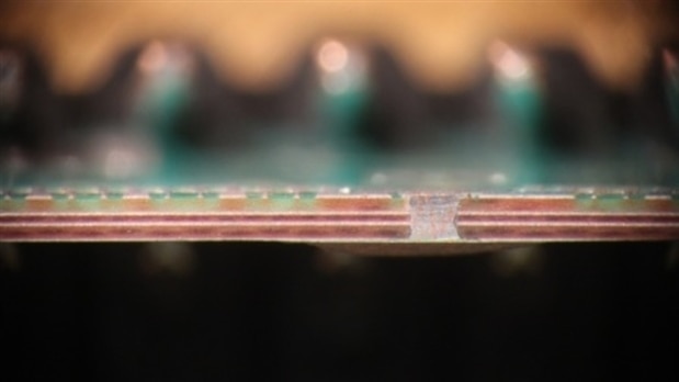
PCB Cameras

(Image credit: AVNETAVNET)
Printed circuit board (PCB) cameras are another recent innovation that helps simplify board design by incorporating image sensors directly into the design, such as those found in smartphones and surveillance systems. Board cameras are typically digital (CCD, CMOS, CID, and more) and have their optical components, such as the aperture, lens, and image sensor, attached directly to a printed circuit board with included input/output options. Images and video are relayed via I/O on the PCB to displays and monitors, and can be used for any number of applications, including machine vision (AI), home security, autonomous vehicles, and more. This 96Boards mezzanine card by AVNET features two Polight IAS-compatible imaging modules based on imaging sensors from ON Semiconductor. These MIPI sensor modules interface to an AP1302 imaging coprocessor. Designed as an expansion card for the Ultra96-V2 single board computer, this card is designed to conform with the 96Boards standard allowing it to also be used with a variety of other 96Boards products.
High-Speed PCBs

(Image credit: Pixabay)
Multi-core processors that run at 4GHz or higher, M.2 NVMe drives, Wi-Fi 6, and 5G are just a few of the technologies pushing the speed envelope, and PCBs have to follow suit to maintain their integrity. High-speed PCBs are those that can provide a maximum bandwidth of digital signals while mitigating any adverse effects, such as electromagnetic interference (EMI), impedance discontinuities, temperature issues, noise, and more. While multilayer PCBs still retain the crown when it comes to high-speed design, others turn to 3D printed materials with customized interconnect geometry to overcome bottlenecking and signal distortion.
In this case, inkjet printing using a dielectric substrate and conductive traces created from nanoparticle inks are deposited to form a thin film of material that's slowly built up to form a multilayered PCB. Using this technique eliminates copper etching, creating a smooth interface between conductors and the substrate, helping to mitigate DC loss. The dielectric material eliminates the fiber weave pattern found in traditional PCBs, eliminates skew and directional effects, and 3D printed polymers can be modified and doped with other materials to optimize frequency ranges for a tunable bandwidth.
Flexible PCBs

(Image credit: Chris Lohr/Air Force Research Laboratory via YouTube)
One of the most remarkable innovations over the last decade is flexible PCBs, which can flex and bend without damaging the ICs or traces, as the name implies. These use a malleable substrate, often polyimide-based, and can be used to interconnect devices or incorporate all the necessary electronics as well. Flexible PCBs have been used to design flexible displays, wearable medical devices that conform to the skin's natural shape, and even robotic actuators.
A recent discovery made by chemical engineers from the Air Force Research Laboratory has produced a flexible, stretchable material that stays conductive and doesn't change resistance. Known as PolyLMN (Polymerized Liquid Metal), the liquid metal can be sprayed on a substrate through a laser-cut stencil to create traces. The key to its flexibility lies in the individual particles of liquid metal, which are enclosed in a shell resembling a balloon. Each particle is tethered to another, like a chain-link, through a polymerization process. As the particles are strained, they tear open and liquid metal is released, maintaining the connection.
Embedded Passive Components

(Image credit: PV Nano Cell)
Embedded passives are resistors, capacitors, inductors, micro-striplines, and other passive electronic components sandwiched between dielectric layers of a substrate. For PCBs, this helps reduce the board assembly's size, minimizes electrical path lengths, and reduces load fluctuations and noise within the system. Manufacturing PCBs with embedded passives isn't new, but some companies and academic institutions have advanced the process to new levels, including redesigning the passives themselves.
PV Nano Cell, in partnership with ProFactor GmbH, is able to print embedded passive components, including silver and carbon-based resistors and capacitors, within PCB layers for smaller and higher-performing devices. The technique involves using an inkjet printer to print embedded conductive traces, resistors, capacitors, and coils during the PCB printing process, leaving only the necessary components on the surface.
PCBs for Superconducting Applications
(Image credit: Omni Circuit Boards)
Typical PCBs use copper traces and interconnects, which can tolerate a wide temperature gamut in most applications, but aluminum beats copper when it comes to cryogenic environments. D-Wave Systems needed a PCB that could handle temperatures as low as 500 milliKelvins for their supercomputer. Omni Circuit Boards took up that challenge, and successfully designed a PCB that uses a micro-foil material constructed of a 40 µm core of aluminum with a 5 µm electro-deposited layer of copper laminated onto a non-conductive substrate. This PCB also uses aluminum-on-aluminum wire-bond pads and solder-on-aluminum joints, and can handle the cryogenic temperature cycles without fracturing the wire bonds.
Autoplacers for easy PCB Design

(Image credit: FRIEDRICH)
Innovation doesn't come in hardware alone; software also plays the lead role when it comes to design. Some CAD platforms offer autoplacers, programs that provide an alternative to autorouters, which optimally place components based on constraints and other criteria. Autoplacers can place components on either side of the PCB by size, or even by the component name. They can also calculate spaces between components and the shortest distance of the signal tracks during placement. Some autoplacers can place packages by schematic symbols, complete with traceroutes added during board orientation, making designing PCBs easier and less time-consuming.
Biodegradable/Eco-Friendly PCBs

(Image credit: Vellore Institute of Technology)
It's estimated that US consumers and businesses discarded 2.37 million tons of e-waste in 2009, and that number continues to grow, not only in the US but worldwide. To help lower those numbers, engineers have been designing PCBs that are biodegradable and decompose over time. To that end, researchers from the Vellore Institute of Technology have designed an alternative material to traditional PCB substrates. Created from banana fiber and wheat gluten composite, the material has a dielectric constant of between 2 to 36, which is well within the range of traditional PCBs and some electronic components. Surprisingly, the biocomposite was also able to dissipate up to 450C of heat and showed no deterioration in performance, even in high humidity environments.
As technology continues to evolve to become faster and more energy-efficient, PCBs are the catalyst for that exponential growth. Researchers and engineers are continually looking to expand their capabilities to handle next-gen devices and electronics, which has led to faster and easier assembly with hundreds of components at reduced manufacturing times. We will undoubtedly continue to see innovations and designs utilizing the latest advanced materials over the next decade that will surpass what we see today, as demand for the latest technology continues to grow.
Top Comments