


Tech Spotlight Summer of FPGAs:
Main Agenda | Lattice | Tech Connection | FPGA Group | Related Poll | Participate in the Discussion
sponsored by

Introduction
Emerging applications such as AI for IoT, 5G communications, industrial, automotive, and security continue to redefine hardware needs for developers. As Edge devices incorporate more cameras and sensors to enable their various AI/ML capabilities, embedded vision becomes one of the most vital elements of autonomous system design. More of the processing involved in embedded vision is moving from the server to Edge devices to reduce data latency and increase data privacy. Edge devices, however, must meet strict design requirements around small form factor, high reliability, and low power consumption.
FPGAs process data in a parallel fashion, which typically provides higher performance at lower power than microcontrollers (which process data serially). This makes them a compelling silicon platform for use in mission-critical systems operating at the Edge. In this Tech Spotlight, we discuss how field programmable gate array (FPGA) technologies benefit Edge computing systems and satisfy their demanding requirements.
| What is Embedded Vision? Embedded vision is the integration of a camera and processing board, rather than a camera and a PC. Embedded vision systems move the processing of images and video from a PC to the device, reducing size, power consumption, and cost, making possible a new class of devices that can see and think. Currently, embedded vision is used in a wide variety of intelligent applications, such as facial recognition, autonomous vehicles, and factory automation |
|---|
The Role of FPGAs in Emerging Applications
FPGAs benefit from an inherent parallel architecture to run their operations; they generally do not rely on one process to finish in order to run another. FPGA designs can be also be reconfigured ‘in the field’ which differentiates it from an ASIC (application specific integrated circuit), whose algorithms are “frozen in silicon.”
In addition to their programmable fabric, FPGAs contain memory blocks, either volatile or non-volatile, and potentially thousands of digital signal processing (DSP) units. Conversely, microprocessor units (MPUs) appear to be blazing fast, as their system clocks run at 2.4 GHz or higher; however, the sequential nature of their processing can translate into higher latencies. Additionally, MPUs tend to consume more power and generate heat. In general, FPGAs run cooler, consume less power, and their parallel nature gives them a latency advantage in many situations.
Overview of the Nexus Platform
The Lattice Nexus FPGA platform uses 28 nm fully depleted silicon-on-insulator (FD-SOI) semiconductor manufacturing technology. The “insulator” in FD-SOI refers to an ultra-thin oxide layer placed on top of the base silicon. The transistor channel is built on a very thin silicon film, which, because of its thinness, does not require channel doping. Doping is the process of introducing small quantities of an impurity (with N or P-type ions) to change electrical conductivity characteristics. Many semiconductors use channel doping to adjust threshold voltage. An FPGA created with the FD-SOI process does not require doping, and is therefore “fully depleted.”
Soft errors are caused by naturally occurring radiation events and can disrupt normal operation of a chip. Soft error rate (SER) is the specification used to measure soft errors. The buried oxide layer in the Nexus FPGAs has the benefit of blocking most of the radiation particles from contacting the substrate. This allows for a significant reduction in soft errors, which is a requirement for mission critical applications, such as automotive or industrial, and particularly in aerospace, where radiation is a greater concern. Nexus platform FPGAs have an SER up to 100 times lower than similar competing devices.
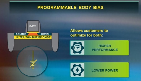
Figure 1: Lattice Nexus Platform Circuit Architecture
Source: https://www.latticesemi.com/view_document?document_id=52906
Lattice Semiconductor
Shop our wide variety of FPGAs, CPLDs, PALs, GALs, and development kits from Lattice.
Don't forget to take our poll.
The FD-SOI process supports a programmable body bias (shown in Figure 1), which allows the FPGA to operate in either a high-performance mode or a low-power mode, depending on the needs of the application. This is made possible by the buried oxide layer, which reduces parasitic current leakage and allows high biasing voltages. Developers can switch between high-performance and low-power modes via software, allowing them to choose the ideal balance of performance and power consumption, depending on their needs. According to Lattice, FPGAs manufactured on the Nexus platform have up to 75% lower power consumption than competing FPGAs of a similar class.
The Nexus FPGA platform architecture uses larger blocks of RAM and optimized DSP blocks than previous platforms. This allows developers to move DSP-intensive processing, like AI inferencing algorithms, from the cloud to the device. Nexus FPGAs deliver twice the performance of earlier Lattice FPGAs while consuming half the power. This enables local Edge AI inferencing at low power for applications such as ADAS systems, smart doorbells, and industrial robots.
Introducing CrossLink-NX
The Lattice CrossLink-NX family of low-power FPGAs is built on the Lattice Nexus FPGA platform, using low-power 28 nm FD-SOI technology. CrossLink-NX FPGAs are optimized for Embedded Vision applications and have the necessary resources to process multiple video streams and perform AI compute functions in real time. They are also capable of bridging legacy and modern interfaces; a key application for enabling machine vision applications in legacy systems.
CrossLink-NX FPGAs feature higher memory-to-logic ratio, optimized DSPs, and faster I/Os than similar competing FPGAs, enabling them to process video data using AI algorithms. CrossLink-NX FPGAs provide highly reliable performance to industrial, automotive, and other mission-critical applications. Since the CrossLink-NX family of devices is pin-compatible, the same design can be used for many applications, and performance boosts can be given to future versions of devices with a simple chip swap.
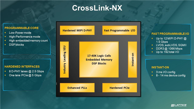
Figure 2: CrossLink-NX Block Diagram
Source: https://www.latticesemi.com/view_document?document_id=52840
As shown in Figure 2, the CrossLink-NX FPGA family supports a variety of hardware and software interfaces like MIPI D-PHY (CSI-2, DSI), LVDS, SLVS, subLVDS, PCI Express (Gen1, Gen2), SGMII (Gigabit Ethernet), and more.
Development Tools
Solution Stacks
Lattice offers several solution stacks to simplify and accelerate the development of many popular applications based on Lattice FPGAs. These stacks include software tools, IP cores, modular hardware development boards, and software-programmable reference designs and demos. In many cases, fully functioning solutions can be developed with the included source code. Lattice CrossLink-NX FPGAs are compatible with two solution stacks in the Lattice portfolio, Lattice sensAI for AI/ML applications at the Edge and Lattice mVision for embedded vision applications like machine vision.
Lattice Propel
Application development using FPGAs has traditionally relied on expertise in specialized hardware development languages. To make FPGA development accessible to a larger number of developers, Lattice offers Lattice Propel, a GUI-based design environment that lets developers drag and drop IP blocks from an IP library into an FPGA design, outputting a functional design. It features a complete set of graphical and command-line tools to create, analyze, compile, and debug both the hardware and software design of an FPGA-based system.
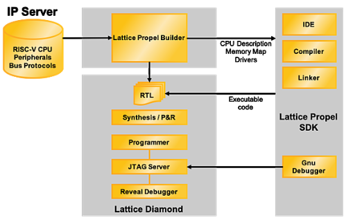
Figure 3: Lattice Propel Design Environment Block Diagram
Source: https://www.latticesemi.com/en/Products/DesignSoftwareAndIP/FPGAandLDS/LatticePropel
As shown in Figure 3, Propel combines two tools, Propel Builder (for IP system integration) and the Propel SDK (for application software development) to form a Propel Design Environment. Propel also integrates with other Lattice design software (Radiant for current products and Diamond for legacy products).
Applications
The Lattice CrossLink-NX FPGAs are specifically designed to perform applications that are commonplace in embedded vision and support high-resolution video in a wide variety of formats and interfaces. We will discuss three commonly needed video applications: Signal Processing, Multiplexing, and Splitting or Duplication.
a. Edge AI and Image Signal Processing
Video-centric applications often require support for the preprocessing of data streams as they move between image sensors to displays, cameras, and application processors (APs). Many systems rely on legacy cameras and displays, which produce data streams that must be translated in real time. Edge AI applications often need to preprocess sensor data before it can be sent to the AP for AI inferencing. Figure 4 is a block diagram of an Edge AI processing system using a CrossLink-NX FPGA to conduct AI inferencing on data before it’s sent to the AP. Figure 5 shows a CrossLink-NX FPGA pre-processing image sensor data before passing it on.
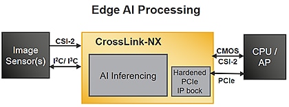
Figure 4: Edge AI processing with a CrossLink-NX FPGA
Source: https://www.latticesemi.com/en/Products/FPGAandCPLD/CrossLink-NX
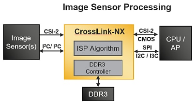
Figure 5: Image signal processing with a CrossLink-NX FPGA
Source: https://www.latticesemi.com/en/Products/FPGAandCPLD/CrossLink-NX
b. Aggregation
Figure 6 illustrates a system where the video streams of up to 11 cameras are merged into one larger video frame, all within the CrossLink-NX FPGA. The FPGA receives MIPI CSI-2 (Camera Serial Interface-2) video data streams from several sources and stitches them into a single larger horizontal video stream, handling any format conversions. DDR3 memory can be incorporated for more memory-intensive processing, such as stitching the data into a larger vertical frame. The resulting stream is sent over fast MIPI D-PHY to a display or processor for additional processing. Potential applications include ADAS systems where data is collected from multiple cameras and/or radar sensors, aggregated, and then forwarded to a processor to make safety decisions, all of it happening in real-time.
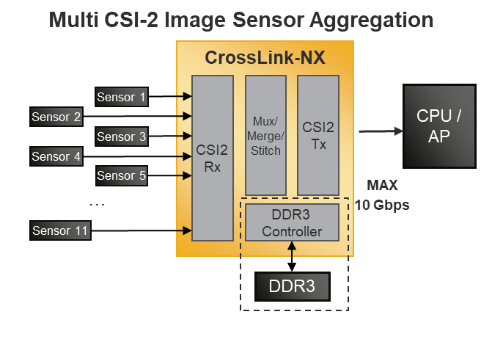
Figure 6: Sensor Aggregation
Source: https://www.latticesemi.com/Products/FPGAandCPLD/CrossLink-NX
c. Splitting or Duplication
Many applications require the splitting or duplication of the video stream coming from a camera, sensor, or display interface. Figure 7 shows the block diagram of a signal split or duplication system. A CrossLink-NX FPGA is programmed to split or duplicate a single high-speed input CSI-2/DSI signal to up to 14 CSI-2/DSI video outputs. Example applications include providing redundancy to sensor data in safety-critical applications or providing multiple video feeds from one or more cameras in video production or industrial environments.
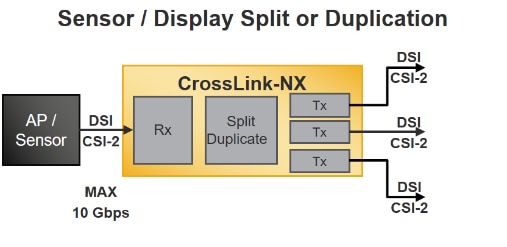
Figure 7: Sensor/Display Split or Duplication
Source: https://www.latticesemi.com/Products/FPGAandCPLD/CrossLink-NX
Conclusion
The Lattice CrossLink-NX FPGA family provides class-leading performance, reliability, and low power consumption for Edge AI/ML and embedded vision applications. With the processing power to handle numerous video feeds, format translations, and AI computations in real-time, CrossLink-NX FPGAs are well-suited for intelligent embedded vision applications that require flexibility, power efficiency, and high performance. The Lattice Propel development environment and the mVision and sensAI solution stacks further simplify and accelerate development of systems based on CrossLink-NX FPGAs.
CrossLink-NX FPGA Development Boards
| LIFCL-40-EVN | LIFCL-VIP-SI-EVN |
|---|---|
Evaluation Board, Crosslink-NX FPGA For More InformationFor More Information |
Sensor Input Board, Crosslink-NX VIP, FPGA For More InformationFor More Information |


