


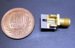
Terahertz modem next to a 10 yen coin. (Via Rohm Semiconductors)
The terahertz waves in industry sit between 100GHz and 10THz. The equipment needed to operate in those heights is large and expensive, but give a bandwidth of 0.1Gbps. This was top of the line until Rohm Semiconductors came out of nowhere touting speeds of 1.5Gbps in the 300GHz band. The 2cm by 1cm device, with an integrated antenna adapter, is the smallest ever made for this level of wireless communication.
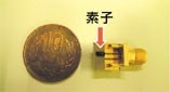

(right) RTD - Resonant Tunneling Diodes house with the integrated antenna. (Via Rohm)
Rohm worked alongside researchers at Osaka University to create the transmission module. The driving chip is only 1.5mm by 3mm. According to Rohm, the modem uses resonant tunneling diodes, oscillator, and a sensing element to achieve a 4x sensitivity boost over current terahertz tech. Four-times Full HD video was shown to be possible during the tests. Which is four-times 4k video, with a 4,096 x 3,112 pixel resolution.
The team claims that more bandwidth can be added to the system without increasing the power demand. Which they clain will boost from 1.5Gbps to a theoretical 30Gbps. The best part is that Rohm will be offering the communication chips at "several hundred yen," or just a few U.S. dollars each. My first thought, how soon will we have these chips in our portable devices?
Cabe
Terahertz radiation range is often referred to as THF, Tremendously High Frequency. (300GHz - 3THz.) What is 10THz then? LHF, Ludicrously High Frequency?
From Rohm: Resonant tunneling diodes (RTD: Resonant Tunneling Diode)
Barrier layer is sufficiently thin structure on either side of the quantum well, electrons in the outer wells can escape through a tunnel barrier. If the incident electron is one barrier, the probability will pass through the barrier and the other corresponds to the quantum levels in the quantum well have been the original form, and increases resonance by the energy of incident electrons. This is the resonance tunneling effect, which was used as a diode.
Barrier layer is sufficiently thin structure on either side of the quantum well, electrons in the outer wells can escape through a tunnel barrier. If the incident electron is one barrier, the probability will pass through the barrier and the other corresponds to the quantum levels in the quantum well have been the original form, and increases resonance by the energy of incident electrons. This is the resonance tunneling effect, which was used as a diode.

