element14 Community
element14 Community
    Register Log In
  • Site
  • Search
  • Log In Register
  • About Us
  • Community Hub
    Community Hub
    • What's New on element14
    • Feedback and Support
    • Benefits of Membership
    • Personal Blogs
    • Members Area
    • Achievement Levels
  • Learn
    Learn
    • Ask an Expert
    • eBooks
    • element14 presents
    • Learning Center
    • Tech Spotlight
    • STEM Academy
    • Webinars, Training and Events
    • Learning Groups
  • Technologies
    Technologies
    • 3D Printing
    • FPGA
    • Industrial Automation
    • Internet of Things
    • Power & Energy
    • Sensors
    • Technology Groups
  • Challenges & Projects
    Challenges & Projects
    • Design Challenges
    • element14 presents Projects
    • Project14
    • Arduino Projects
    • Raspberry Pi Projects
    • Project Groups
  • Products
    Products
    • Arduino
    • Avnet Boards Community
    • Dev Tools
    • Manufacturers
    • Multicomp Pro
    • Product Groups
    • Raspberry Pi
    • RoadTests & Reviews
  • Store
    Store
    • Visit Your Store
    • Choose another store...
      • Europe
      •  Austria (German)
      •  Belgium (Dutch, French)
      •  Bulgaria (Bulgarian)
      •  Czech Republic (Czech)
      •  Denmark (Danish)
      •  Estonia (Estonian)
      •  Finland (Finnish)
      •  France (French)
      •  Germany (German)
      •  Hungary (Hungarian)
      •  Ireland
      •  Israel
      •  Italy (Italian)
      •  Latvia (Latvian)
      •  
      •  Lithuania (Lithuanian)
      •  Netherlands (Dutch)
      •  Norway (Norwegian)
      •  Poland (Polish)
      •  Portugal (Portuguese)
      •  Romania (Romanian)
      •  Russia (Russian)
      •  Slovakia (Slovak)
      •  Slovenia (Slovenian)
      •  Spain (Spanish)
      •  Sweden (Swedish)
      •  Switzerland(German, French)
      •  Turkey (Turkish)
      •  United Kingdom
      • Asia Pacific
      •  Australia
      •  China
      •  Hong Kong
      •  India
      •  Korea (Korean)
      •  Malaysia
      •  New Zealand
      •  Philippines
      •  Singapore
      •  Taiwan
      •  Thailand (Thai)
      • Americas
      •  Brazil (Portuguese)
      •  Canada
      •  Mexico (Spanish)
      •  United States
      Can't find the country/region you're looking for? Visit our export site or find a local distributor.
  • Translate
  • Profile
  • Settings
Publications
  • Learn
  • More
Publications
Blog IBM‘s Nanotube Contact Solution Could Enable 1.8nm Devices
  • Blog
  • Documents
  • Events
  • Files
  • Members
  • Mentions
  • Sub-Groups
  • Tags
  • More
  • Cancel
  • New
Join Publications to participate - click to join for free!
  • Share
  • More
  • Cancel
Group Actions
  • Group RSS
  • More
  • Cancel
Engagement
  • Author Author: GardenState
  • Date Created: 5 Oct 2015 1:55 PM Date Created
  • Views 622 views
  • Likes 0 likes
  • Comments 0 comments
Related
Recommended

IBM‘s Nanotube Contact Solution Could Enable 1.8nm Devices

GardenState
GardenState
5 Oct 2015

image

Silicon transistors have been made smaller year after year, but they are approaching a point of physical limitation. Continuing to shrink the size of the transistor – including the channels and contacts – without compromising performance has become a major technology hurdle..


Researchers have known that carbon nanotube (CNT) chips could provide an answer, greatly improving the capabilities of high performance computers and other devices, The carbon nanotubes form the core of a transistor device whose superior electrical properties promise several generations of technology scaling beyond the physical limits of silicon. The promise of CNTs centers on the fact that electrons in carbon transistors can move more easily than in silicon-based devices, and the ultra-thin body of carbon nanotubes provide additional advantages at the atomic scale


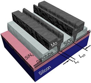
The trouble is as devices become smaller, increased contact resistance for carbon nanotubes has hindered performance gains. Inside a chip, the contacts are the valves that control the flow of electrons from metal into the channels of a semiconductor. As transistors shrink in size, electrical resistance increases within the contacts, which impedes performance


But now IBM researchers say they have found a way to forego traditional contact schemes and have invented a metallurgical process akin to microscopic welding that chemically binds the metal atoms to the carbon atoms at the ends of nanotubes. This ‘end-bonded contact scheme’ is said to allow the contacts to be shrunken down to below 10 nanometers without deteriorating performance of the carbon nanotube devices.


IBM, which had previously shown that carbon nanotube transistors can operate as excellent switches at channel dimensions of less than ten nanometers, says that the new development can overcome contact resistance challenges all the way to the 1.8 nanometer node – four technology generations away, Dario Gil, IBM vice president of Science and Technology characterized the breakthrough as bringing us “a step closer to the goal of a carbon nanotube technology within the decade.”.

  • Sign in to reply
element14 Community

element14 is the first online community specifically for engineers. Connect with your peers and get expert answers to your questions.

  • Members
  • Learn
  • Technologies
  • Challenges & Projects
  • Products
  • Store
  • About Us
  • Feedback & Support
  • FAQs
  • Terms of Use
  • Privacy Policy
  • Legal and Copyright Notices
  • Sitemap
  • Cookies

An Avnet Company © 2025 Premier Farnell Limited. All Rights Reserved.

Premier Farnell Ltd, registered in England and Wales (no 00876412), registered office: Farnell House, Forge Lane, Leeds LS12 2NE.

ICP 备案号 10220084.

Follow element14

  • X
  • Facebook
  • linkedin
  • YouTube