element14 Community
element14 Community
    Register Log In
  • Site
  • Search
  • Log In Register
  • Community Hub
    Community Hub
    • What's New on element14
    • Feedback and Support
    • Benefits of Membership
    • Personal Blogs
    • Members Area
    • Achievement Levels
  • Learn
    Learn
    • Ask an Expert
    • eBooks
    • element14 presents
    • Learning Center
    • Tech Spotlight
    • STEM Academy
    • Webinars, Training and Events
    • Learning Groups
  • Technologies
    Technologies
    • 3D Printing
    • FPGA
    • Industrial Automation
    • Internet of Things
    • Power & Energy
    • Sensors
    • Technology Groups
  • Challenges & Projects
    Challenges & Projects
    • Design Challenges
    • element14 presents Projects
    • Project14
    • Arduino Projects
    • Raspberry Pi Projects
    • Project Groups
  • Products
    Products
    • Arduino
    • Avnet & Tria Boards Community
    • Dev Tools
    • Manufacturers
    • Multicomp Pro
    • Product Groups
    • Raspberry Pi
    • RoadTests & Reviews
  • About Us
  • Store
    Store
    • Visit Your Store
    • Choose another store...
      • Europe
      •  Austria (German)
      •  Belgium (Dutch, French)
      •  Bulgaria (Bulgarian)
      •  Czech Republic (Czech)
      •  Denmark (Danish)
      •  Estonia (Estonian)
      •  Finland (Finnish)
      •  France (French)
      •  Germany (German)
      •  Hungary (Hungarian)
      •  Ireland
      •  Israel
      •  Italy (Italian)
      •  Latvia (Latvian)
      •  
      •  Lithuania (Lithuanian)
      •  Netherlands (Dutch)
      •  Norway (Norwegian)
      •  Poland (Polish)
      •  Portugal (Portuguese)
      •  Romania (Romanian)
      •  Russia (Russian)
      •  Slovakia (Slovak)
      •  Slovenia (Slovenian)
      •  Spain (Spanish)
      •  Sweden (Swedish)
      •  Switzerland(German, French)
      •  Turkey (Turkish)
      •  United Kingdom
      • Asia Pacific
      •  Australia
      •  China
      •  Hong Kong
      •  India
      • Japan
      •  Korea (Korean)
      •  Malaysia
      •  New Zealand
      •  Philippines
      •  Singapore
      •  Taiwan
      •  Thailand (Thai)
      • Vietnam
      • Americas
      •  Brazil (Portuguese)
      •  Canada
      •  Mexico (Spanish)
      •  United States
      Can't find the country/region you're looking for? Visit our export site or find a local distributor.
  • Translate
  • Profile
  • Settings
Publications
  • Learn
  • More
Publications
Blog Nanotechnology helps create 100,000 dpi resolution images
  • Blog
  • Documents
  • Events
  • Files
  • Members
  • Mentions
  • Sub-Groups
  • Tags
  • More
  • Cancel
  • New
Join Publications to participate - click to join for free!
  • Share
  • More
  • Cancel
Group Actions
  • Group RSS
  • More
  • Cancel
Engagement
  • Author Author: Catwell
  • Date Created: 24 Aug 2012 6:03 AM Date Created
  • Views 532 views
  • Likes 1 like
  • Comments 0 comments
  • research
  • test
  • industry
  • hmi
  • image
  • on_campus
  • embedded
  • cabeatwell
  • prototyping
  • measurement
  • university
  • machine_vision
  • sensor
  • innovation
Related
Recommended

Nanotechnology helps create 100,000 dpi resolution images

Catwell
Catwell
24 Aug 2012

image

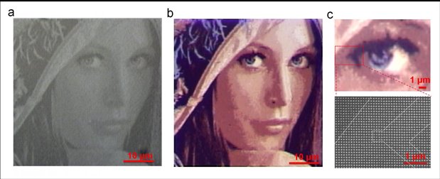
(a) nanostructure base image (b) metal is added to the nano-structure, colours observed (c) enlarged image of the eye's corner (via A*STAR & Nature Technology)


Researchers from A*STAR's Institute of Materials Research and Engineering in Singapore have developed an innovative new way to create images in a much higher resolution. Current laserjet and inkjet printers can produce images in full color at up to 10,000 dots per inch (dpi). The researchers claim that their new method would have a potential limit of creating images at up to 100,000dpi.


The work is said to have been derived from inspiration through the way stained glass is traditionally created. Stained glass is made by mixing tiny fragments of metal into the glass which scatter light passing through it and give the stained glass its color. Similarly, researchers used nanotechnology to precisely pattern metal nanostructures together and created a surface to reflect light of specific colors to create color images.


“Instead of using different dyes for different colours, we encoded colour information into the size and position of tiny metal disks. These disks then interacted with light through the phenomenon of plasmon resonances,” said Dr Joel Yang, the project leader of the research. With the nanostructures placed accordingly, placing the ultra thin metal film over the picture made all the “encoded” colors seem to all appear at once.


The new technique is much more similar to lithography than traditional printing but could possibly be the foundation for the future of the way we create images. Furthermore, researchers stated the technology could be further developed for use in high-resolution reflective color displays and high density optical data storage. Who would have guessed something as old as stained glass would have inspired a new way to create the most high resolution images to date.


Cabe

http://twitter.com/Cabe_e14

  • Sign in to reply
element14 Community

element14 is the first online community specifically for engineers. Connect with your peers and get expert answers to your questions.

  • Members
  • Learn
  • Technologies
  • Challenges & Projects
  • Products
  • Store
  • About Us
  • Feedback & Support
  • FAQs
  • Terms of Use
  • Privacy Policy
  • Legal and Copyright Notices
  • Sitemap
  • Cookies

An Avnet Company © 2026 Premier Farnell Limited. All Rights Reserved.

Premier Farnell Ltd, registered in England and Wales (no 00876412), registered office: Farnell House, Forge Lane, Leeds LS12 2NE.

ICP 备案号 10220084.

Follow element14

  • X
  • Facebook
  • linkedin
  • YouTube