


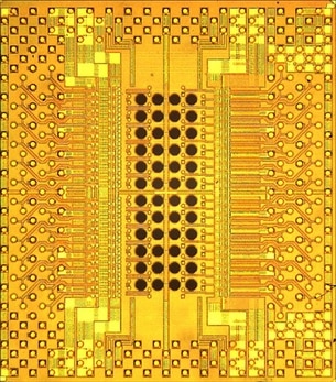
Optochip prototype (via IBM)
Data transfer speeds have increased significantly over the past decade with the introduction of new interfaces, flash-drives, USB 3.0 and SSD’s. These can’t hold a candle to IBM’s new optical chipset which has a transfer rate of 1 terabit per second.
Dubbed ‘Holey Optochip,' the chip-scale transceivers (optical network interfaces) use fiber-optical connections rather than traditional copper leads or wires to move data which amps up the speed considerably. The prototype uses parallel-optics technology that is able to send and receive information at the same time over multiple fiber optic connections. It may be hard to see in the above picture, the IBM researchers used a 90 nanometer CMOS transceiver with 48 optical ‘vias’ (vertical electrical connections) with 24 holes allocated for receivers (photodiode array’s) and the other 24 populated by 850-nm VCSEL’s (lasers). They are then connected to each other using the flip-soldering technique (soldering to the bond pads then mash to the board using an adhesive) which apparently helps make the Holey Optochip fast as well as easy to produce by conventional means.
So, are we likely to see the Holey Optochip integrated into Motherboards or other electronics in the near future? Perhaps, but not likely, as IBM has other light related projects gathering dust in their lab closet. It may end up on the pile with projects such as the ‘CMOS integrated Silicon Nanophotonics’ project (2010), which paired both electrical and optical pathways on the same chip or the ‘Mach-Zehnder elctro-optic modulator’ which was to help multiple CPU cores on a single die communicate with each other using fiber-optics. Then again IBM has a way of surprising people when they’re least expecting it.
Cabe
