element14 Community
element14 Community
    Register Log In
  • Site
  • Search
  • Log In Register
  • Community Hub
    Community Hub
    • What's New on element14
    • Feedback and Support
    • Benefits of Membership
    • Personal Blogs
    • Members Area
    • Achievement Levels
  • Learn
    Learn
    • Ask an Expert
    • eBooks
    • element14 presents
    • Learning Center
    • Tech Spotlight
    • STEM Academy
    • Webinars, Training and Events
    • Learning Groups
  • Technologies
    Technologies
    • 3D Printing
    • FPGA
    • Industrial Automation
    • Internet of Things
    • Power & Energy
    • Sensors
    • Technology Groups
  • Challenges & Projects
    Challenges & Projects
    • Design Challenges
    • element14 presents Projects
    • Project14
    • Arduino Projects
    • Raspberry Pi Projects
    • Project Groups
  • Products
    Products
    • Arduino
    • Avnet & Tria Boards Community
    • Dev Tools
    • Manufacturers
    • Multicomp Pro
    • Product Groups
    • Raspberry Pi
    • RoadTests & Reviews
  • About Us
  • Store
    Store
    • Visit Your Store
    • Choose another store...
      • Europe
      •  Austria (German)
      •  Belgium (Dutch, French)
      •  Bulgaria (Bulgarian)
      •  Czech Republic (Czech)
      •  Denmark (Danish)
      •  Estonia (Estonian)
      •  Finland (Finnish)
      •  France (French)
      •  Germany (German)
      •  Hungary (Hungarian)
      •  Ireland
      •  Israel
      •  Italy (Italian)
      •  Latvia (Latvian)
      •  
      •  Lithuania (Lithuanian)
      •  Netherlands (Dutch)
      •  Norway (Norwegian)
      •  Poland (Polish)
      •  Portugal (Portuguese)
      •  Romania (Romanian)
      •  Russia (Russian)
      •  Slovakia (Slovak)
      •  Slovenia (Slovenian)
      •  Spain (Spanish)
      •  Sweden (Swedish)
      •  Switzerland(German, French)
      •  Turkey (Turkish)
      •  United Kingdom
      • Asia Pacific
      •  Australia
      •  China
      •  Hong Kong
      •  India
      • Japan
      •  Korea (Korean)
      •  Malaysia
      •  New Zealand
      •  Philippines
      •  Singapore
      •  Taiwan
      •  Thailand (Thai)
      • Vietnam
      • Americas
      •  Brazil (Portuguese)
      •  Canada
      •  Mexico (Spanish)
      •  United States
      Can't find the country/region you're looking for? Visit our export site or find a local distributor.
  • Translate
  • Profile
  • Settings
Publications
  • Learn
  • More
Publications
Blog Semiconductors grown on graphene set to be commercialized
  • Blog
  • Documents
  • Events
  • Files
  • Members
  • Mentions
  • Sub-Groups
  • Tags
  • More
  • Cancel
  • New
Join Publications to participate - click to join for free!
  • Share
  • More
  • Cancel
Group Actions
  • Group RSS
  • More
  • Cancel
Engagement
  • Author Author: Catwell
  • Date Created: 8 Oct 2012 6:56 PM Date Created
  • Views 464 views
  • Likes 1 like
  • Comments 1 comment
  • research
  • graphene
  • industry
  • on_campus
  • Design
  • cabeatwell
  • prototyping
  • measurement
  • semiconductor
  • university
  • power
  • energy
  • innovation
Related
Recommended

Semiconductors grown on graphene set to be commercialized

Catwell
Catwell
8 Oct 2012

image

Graphene Nano-wire on graphene concept (via Crayonano)


With all of the latest developments regarding graphene production and applications, could we finally be on the verge of running 3000GHz CPU’s on our systems and mobile devices? According to a team of scientists from the Norwegian University of Science and Technology, that day might be closer than you think. Their development is a semiconductor nano-wire that has been grown on the metamaterial, which could be described as tiny, yet powerful, electronic mushrooms. This is the first commercialized  semiconductor grown on graphene.


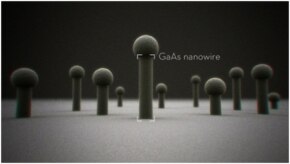
To create their GaAs nanowires the team used a process known as molecular beam epitaxy (MBE) which is used to deposit crystals in a high-vacuum chamber to create semiconductor films. However in this case the scientists substituted gallium atoms and arsenic molecules rather than silicon. These gallium atoms were bombarded against an atom-thick graphene surface where they then bonded to the substrate. Over time, the gallium atoms combine together to form tiny droplets, which arrange themselves with the graphene’s hexagonal lattice structure. The group then introduced the arsenic molecules to the mix which would sink to the bottom of the gallium droplets which then combined with each-other to form a crystalline structure on the point of contact with the graphene. As more arsenic molecules and gallium atoms combine the resulting crystalline structure continues to grow into a nano-wire with the initial gallium droplet perched at the top. After a few minutes the semiconductor nano-wire fabrication process is finished with an end-result of a pliable transparent base that could be adapted to new, and relatively cheap, solar cells and LED’s. The scientists state that their findings aren’t meant as a new product but rather a new method for fabrication of graphene-based semiconductor devices. This production method could introduce flexible touch screens for mobile devices, such as a smartphone screen that wraps around your wrist or implemented into solar-cells that could be fabricated into the windows of your home.


You don't have permission to edit metadata of this video.
Edit media
x
image
Upload Preview
image


Cabe

http://twitter.com/Cabe_e14

  • Sign in to reply
  • DAB
    DAB over 13 years ago

    Since the Graphene devices are in their infancy, it will be interesting to see what kind of capability the devices have.

    I could see many hours in a lab just exploring the capability and the unexpected features that arise.


    Very interesting development.


    DAB

    • Cancel
    • Vote Up 0 Vote Down
    • Sign in to reply
    • More
    • Cancel
element14 Community

element14 is the first online community specifically for engineers. Connect with your peers and get expert answers to your questions.

  • Members
  • Learn
  • Technologies
  • Challenges & Projects
  • Products
  • Store
  • About Us
  • Feedback & Support
  • FAQs
  • Terms of Use
  • Privacy Policy
  • Legal and Copyright Notices
  • Sitemap
  • Cookies

An Avnet Company © 2026 Premier Farnell Limited. All Rights Reserved.

Premier Farnell Ltd, registered in England and Wales (no 00876412), registered office: Farnell House, Forge Lane, Leeds LS12 2NE.

ICP 备案号 10220084.

Follow element14

  • X
  • Facebook
  • linkedin
  • YouTube