


(Left) Breakdownn of the printed substrate (Right) Tunneling microscope view of silicene (via PAtrick Vogt)
Graphene has been widely touted as the future replacement of silicon in electrical applications. In a turn of tables, element 14 (silicon) returns as a two dimensional allotrope known as "silicene." A collaborative effort between Berlin's Technical University and Aix-Marseille University led by Patrick Vogt were successful in creating a hexagonal sheet of silicon which is only 1 atom thick.
While graphene is an excellent superconductor in itself, it does not get along with silicon all that well due to integration/band-gap problems concerning the two materials. Whereas silicon (Si) based silicene has a honeycomb-lattice structure that allows electrons to ‘jump’ with relative ease back and forth which makes for a novel transistor on the small scale. To synthesize the silicene sheet, the scientists condensed silicon vapor onto a silver substrate. Then it was verified using a scanning tunneling microscope with an angular-resolved photoemission spectroscopy (ARPES), which is a scientific term for observing the distribution of electrons on a very, very small scale. The results showed silicene followed suit with predicted characteristics. Keep in mind, this does not mean an atom sized silicon transistor can be made. Silicon components are somewhat unpredictable smaller than 10 nano-meters.
Four other groups have claimed to accomplish the same feat using the same methods, but this team was the first to back it up with clear (albeit tiny) proof. The next step the team wants to pursue is to grow silicene on insulated substrates to measure its electrical properties which would give them better ideas as to how it could be incorporated into future electronics.
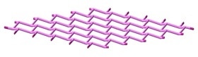
Silicene concept latice (via wikipedia)
Cabe
