element14 Community
element14 Community
    Register Log In
  • Site
  • Search
  • Log In Register
  • Community Hub
    Community Hub
    • What's New on element14
    • Feedback and Support
    • Benefits of Membership
    • Personal Blogs
    • Members Area
    • Achievement Levels
  • Learn
    Learn
    • Ask an Expert
    • eBooks
    • element14 presents
    • Learning Center
    • Tech Spotlight
    • STEM Academy
    • Webinars, Training and Events
    • Learning Groups
  • Technologies
    Technologies
    • 3D Printing
    • FPGA
    • Industrial Automation
    • Internet of Things
    • Power & Energy
    • Sensors
    • Technology Groups
  • Challenges & Projects
    Challenges & Projects
    • Design Challenges
    • element14 presents Projects
    • Project14
    • Arduino Projects
    • Raspberry Pi Projects
    • Project Groups
  • Products
    Products
    • Arduino
    • Avnet & Tria Boards Community
    • Dev Tools
    • Manufacturers
    • Multicomp Pro
    • Product Groups
    • Raspberry Pi
    • RoadTests & Reviews
  • About Us
  • Store
    Store
    • Visit Your Store
    • Choose another store...
      • Europe
      •  Austria (German)
      •  Belgium (Dutch, French)
      •  Bulgaria (Bulgarian)
      •  Czech Republic (Czech)
      •  Denmark (Danish)
      •  Estonia (Estonian)
      •  Finland (Finnish)
      •  France (French)
      •  Germany (German)
      •  Hungary (Hungarian)
      •  Ireland
      •  Israel
      •  Italy (Italian)
      •  Latvia (Latvian)
      •  
      •  Lithuania (Lithuanian)
      •  Netherlands (Dutch)
      •  Norway (Norwegian)
      •  Poland (Polish)
      •  Portugal (Portuguese)
      •  Romania (Romanian)
      •  Russia (Russian)
      •  Slovakia (Slovak)
      •  Slovenia (Slovenian)
      •  Spain (Spanish)
      •  Sweden (Swedish)
      •  Switzerland(German, French)
      •  Turkey (Turkish)
      •  United Kingdom
      • Asia Pacific
      •  Australia
      •  China
      •  Hong Kong
      •  India
      • Japan
      •  Korea (Korean)
      •  Malaysia
      •  New Zealand
      •  Philippines
      •  Singapore
      •  Taiwan
      •  Thailand (Thai)
      • Vietnam
      • Americas
      •  Brazil (Portuguese)
      •  Canada
      •  Mexico (Spanish)
      •  United States
      Can't find the country/region you're looking for? Visit our export site or find a local distributor.
  • Translate
  • Profile
  • Settings
Publications
  • Learn
  • More
Publications
Blog Stretchable nanotube transistor material from DOE Berkely, a touch interface
  • Blog
  • Documents
  • Events
  • Files
  • Members
  • Mentions
  • Sub-Groups
  • Tags
  • More
  • Cancel
  • New
Join Publications to participate - click to join for free!
  • Share
  • More
  • Cancel
Group Actions
  • Group RSS
  • More
  • Cancel
Engagement
  • Author Author: Catwell
  • Date Created: 15 Dec 2011 8:15 PM Date Created
  • Views 398 views
  • Likes 0 likes
  • Comments 0 comments
  • transistor
  • hmi
  • cell_phone
  • on_campus
  • embedded
  • doe
  • berkely
  • cabeatwell
  • prototyping
  • electronic_products
  • university
  • medical
  • sensor
  • innovation
Related
Recommended

Stretchable nanotube transistor material from DOE Berkely, a touch interface

Catwell
Catwell
15 Dec 2011
image
A baseball covered in the DOE Berkely stretchable thin film transistor array material (via DOE Berkely)
 
Many researchers are part of a race to creating stretchable/bendable electronics. Seamlessly integrated wearable electronics is now an inevitability. The U.S. Department of Energy (DOE) is no slouch in this area either with their latest development, large-area  carbon-nanotube thin film transistor networks.
 
The material was developed at the Lawrence Berkely National Laboratory. The high charge mobility outstrips the capabilities of its organic counterparts. The team's first application was to take transistor network, they dubbed "e-skin," and use it as a touch interface.
 
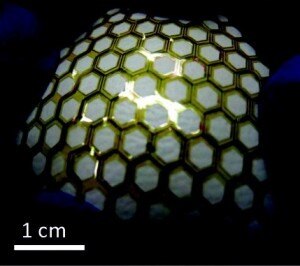
A major issue the team tackled in this project was the carbon nanotube's low band-gap ratio (the on/off ratio, as the team called it). To defeat the low on/off ratio of the material the team had to make the purest solution of single-wall carbon nanotubes (SWNT) as possible. They make a solution that was 99% semiconductor SWNT. Applying this solution to a polymide substrate created the base material. To make it flexible, a hexagonal (honeycomb) shape was laser-cut into the sheets at a pitch of 3.3mm and a hole-side lenth between 1 - 1.85mm. 
 
The paper's co-author Toshitake Takahashi explained the purpose on the holes, "The degree to which the substrate could be stretched increased from 0 to 60-percent as the side length of the hexagonal holes increased to 1.85 mm... In the future, the degrees of stretchability and directionality should be tunable by either changing the hole size or optimizing the mesh design.”
 
The final prototype was a 24 square centimeter "sensor pixel" array. The image below shows the pressure indication map of an "L" shaped object on top of the material. Max pressure of 15 kilo Pascals was sensed.
image
(via DOE Berkely)

 
Takahashi stated that using this array could make for a good touch input backplane for flexible displays in the near future. A common mantra spoken by many in the industry.
 
Cabe
http://twitter.com/Cabe_e14
 
More projects in the flextronics industry:
Transparent graphene transistor material stretches beyond all others
Molybdenite to replace silicon, and the 3-atom thick transistor
Cotton transistor and wearable electronics
Flexible memory breaks through flex limitations
Coiled nanowires could help with stretchable electronics
Stretchable silicon to make ‘smarter’ sports apparel
  • Sign in to reply
element14 Community

element14 is the first online community specifically for engineers. Connect with your peers and get expert answers to your questions.

  • Members
  • Learn
  • Technologies
  • Challenges & Projects
  • Products
  • Store
  • About Us
  • Feedback & Support
  • FAQs
  • Terms of Use
  • Privacy Policy
  • Legal and Copyright Notices
  • Sitemap
  • Cookies

An Avnet Company © 2025 Premier Farnell Limited. All Rights Reserved.

Premier Farnell Ltd, registered in England and Wales (no 00876412), registered office: Farnell House, Forge Lane, Leeds LS12 2NE.

ICP 备案号 10220084.

Follow element14

  • X
  • Facebook
  • linkedin
  • YouTube