element14 Community
element14 Community
    Register Log In
  • Site
  • Search
  • Log In Register
  • Community Hub
    Community Hub
    • What's New on element14
    • Feedback and Support
    • Benefits of Membership
    • Personal Blogs
    • Members Area
    • Achievement Levels
  • Learn
    Learn
    • Ask an Expert
    • eBooks
    • element14 presents
    • Learning Center
    • Tech Spotlight
    • STEM Academy
    • Webinars, Training and Events
    • Learning Groups
  • Technologies
    Technologies
    • 3D Printing
    • FPGA
    • Industrial Automation
    • Internet of Things
    • Power & Energy
    • Sensors
    • Technology Groups
  • Challenges & Projects
    Challenges & Projects
    • Design Challenges
    • element14 presents Projects
    • Project14
    • Arduino Projects
    • Raspberry Pi Projects
    • Project Groups
  • Products
    Products
    • Arduino
    • Avnet & Tria Boards Community
    • Dev Tools
    • Manufacturers
    • Multicomp Pro
    • Product Groups
    • Raspberry Pi
    • RoadTests & Reviews
  • About Us
  • Store
    Store
    • Visit Your Store
    • Choose another store...
      • Europe
      •  Austria (German)
      •  Belgium (Dutch, French)
      •  Bulgaria (Bulgarian)
      •  Czech Republic (Czech)
      •  Denmark (Danish)
      •  Estonia (Estonian)
      •  Finland (Finnish)
      •  France (French)
      •  Germany (German)
      •  Hungary (Hungarian)
      •  Ireland
      •  Israel
      •  Italy (Italian)
      •  Latvia (Latvian)
      •  
      •  Lithuania (Lithuanian)
      •  Netherlands (Dutch)
      •  Norway (Norwegian)
      •  Poland (Polish)
      •  Portugal (Portuguese)
      •  Romania (Romanian)
      •  Russia (Russian)
      •  Slovakia (Slovak)
      •  Slovenia (Slovenian)
      •  Spain (Spanish)
      •  Sweden (Swedish)
      •  Switzerland(German, French)
      •  Turkey (Turkish)
      •  United Kingdom
      • Asia Pacific
      •  Australia
      •  China
      •  Hong Kong
      •  India
      •  Korea (Korean)
      •  Malaysia
      •  New Zealand
      •  Philippines
      •  Singapore
      •  Taiwan
      •  Thailand (Thai)
      • Americas
      •  Brazil (Portuguese)
      •  Canada
      •  Mexico (Spanish)
      •  United States
      Can't find the country/region you're looking for? Visit our export site or find a local distributor.
  • Translate
  • Profile
  • Settings
Publications
  • Learn
  • More
Publications
Blog The 2D semiconductor
  • Blog
  • Documents
  • Events
  • Files
  • Members
  • Mentions
  • Sub-Groups
  • Tags
  • More
  • Cancel
  • New
Join Publications to participate - click to join for free!
  • Share
  • More
  • Cancel
Group Actions
  • Group RSS
  • More
  • Cancel
Engagement
  • Author Author: Catwell
  • Date Created: 14 Nov 2011 9:50 PM Date Created
  • Views 342 views
  • Likes 0 likes
  • Comments 0 comments
  • fabrication
  • quantum
  • alternative_energy
  • transistor
  • on_campus
  • embedded
  • cabeatwell
  • engineering
  • university
  • innovation
Related
Recommended

The 2D semiconductor

Catwell
Catwell
14 Nov 2011
image
2D circuit photographs and bandgap chart. (via the group's report on Nano Letter.)
 
 
So thin that they call it two dimensional, researchers from the University of California, Berkeley, has developed a new class of semiconductor. Quantum confinement is at the heart of the development, where the electrical and optical properties of an unconfined bulk semiconductor change as the size is reduced. The biggest benefit of the discovery comes in the fact the conductors can be applied to any substrate.
 
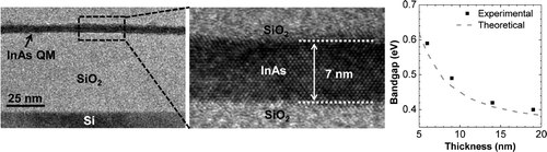
The tech is dubbed Quantum Membranes (QM). To fabricate the conductor, indium arsenide is first grown on Gallium Antimonide (GaSb) or Aluminum Gallium Antimonide (AlGaSb). The bottom layers are removed, leaving the indium arsenide conductors, in whatever shape was originally formed. The conductors can then be placed on any substrate desired. This is somewhat of a elaborate trick to get material compatibility. The electron mobility of the QM is not dependent on electrical fields applied at all but very high fields. The result is used in quantum electrical and optical applications, where graphene was predominantly used. The added benefit of the new conductor over graphene is the bandgap of the material. Graphene hovers around 30eV while this indium arsenide conductor can get lower than 0.4eV.
 
Researchers on the project, led by Ali Javey, claim that this new semiconductor will give  unprecedented data on how quantum confined materials operate. Which, of course, will soon lead to further tweaking and new materials.
 
Cabe
http://twitter.com/Cabe_e14
  • Sign in to reply
element14 Community

element14 is the first online community specifically for engineers. Connect with your peers and get expert answers to your questions.

  • Members
  • Learn
  • Technologies
  • Challenges & Projects
  • Products
  • Store
  • About Us
  • Feedback & Support
  • FAQs
  • Terms of Use
  • Privacy Policy
  • Legal and Copyright Notices
  • Sitemap
  • Cookies

An Avnet Company © 2025 Premier Farnell Limited. All Rights Reserved.

Premier Farnell Ltd, registered in England and Wales (no 00876412), registered office: Farnell House, Forge Lane, Leeds LS12 2NE.

ICP 备案号 10220084.

Follow element14

  • X
  • Facebook
  • linkedin
  • YouTube