


FPGAs or field-programmable gate array are becoming more and more popular it seems. Over the last year I have seen an increase in people asking what FPGA kit should they buy, which languages should they learn, VHDL or Verilog? There are lots of questions and lots of answers. So to deal with that I am starting a series of blog posts here on DIT to look at how to get started with FPGAs - starting with what a FPGA really is.
I started in electronics before FPGA’s really came along and when we were still building circuits out of 4000 series and 74LSxx chips. These were just for glue logic that we needed to interface microprocessors to RAM and ROM etc. But there was only so much you could get in an IC and it was not long before digital engineers were looking for other ways to get lots of logic inside a single chip. More importantly this had to be the logic we wanted - programmed for our needs. So we started using EEPROMS and I have written a separate blog about how we used these and GAL chips before FPGAs came along.
So FPGAs are the chip manufactures answer to our need for large amount of logic in one chip but not the first. There are also chips called CPLDs or Complex Programmable Logic Device. The most common and famous chip being the Altera MAX3000EEUP+ and 7000 series. From a beginners point of view these chips look very much the same. However at a top level the differences are as follows; CPLDs can be programmed once (or repeatably) like a Flash chip and store their configuration, FPGAs, however, are blank on power up and need a device to upload the configuration every time. CPLDs typically have lower gate counts and this is the major difference that most engineers see. CPLDs are basically less flexible internally in the way the logic blocks are connected together but have the advantage of being more predictable on timing. FPGAs however have greater connections and allow for more complex systems. The other great advantage FPGAs now have over early chips are the built in features. These features include RAM logic, PLL (Phase Lock Loops) for generating difference clock frequencies and pre-built logic like adders and other math blocks. These give FPGAs the greater power and flexibility and I guess is why so many people now want to use them.
At the base level inside each FPGA is a block of logic called a LAB, Logic Array Block or sometime called a CLB (Configurable Logic Block). These blocks are then made up of three key elements; a Look Up Table (LUT), a Full Adder and a D-Type flip-flop. There are also a number of bypass Multiplexers (MUX) which we can consider as bypass switches.
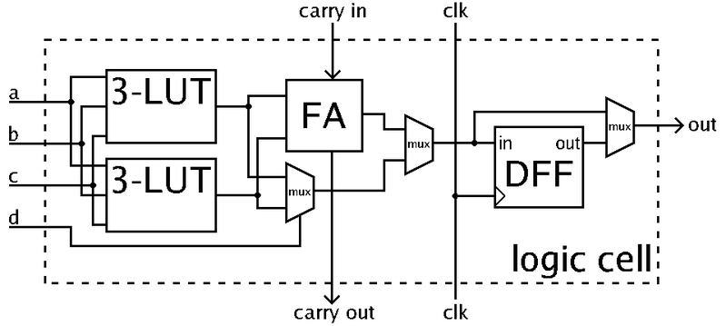
The LUT is nothing more than what I have described in my blog about using EEPROMS. They have a number of inputs which is used to address a register inside a table, this table contains a number of bits which are programmable and then output to the next stage. Most common designs with have two LUTs with something like three input each and output a single bit each. However like all features in FPGAs this differs from manufacture to manufactures as some now have six inputs each.
The next stage is the Full Adder that will normally have a bypass MUX or switch in front and behind it. This allows for the output of the LUTs to either go though the adder or not. The Adder by the way will also have a carry in and out allowing lots of LABs to be connected together to make large adders and counters.
The last stage is a D-Type flip flop that takes its input either from the LUT or Full Adder dependent on the switch settings. It will also have access to the system clock lines. To allow for either synchronous or asynchronous configurations as well as storage. The final output will be a single logic bit that then reaches out into the matrix of connections.
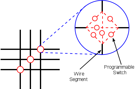
This matrix of connecting wires run between each LAB and themself contain programmable switches. These switches allows for the routing of the signals around the chip as well as to and from each LAB. At a architecture level FPGAs are very complex and if we had to figure out all these connections and setting alone then it would takes weeks to do the most simple of circuits.
Thankfully the manufactures have supplied us with tools to make this easier to do. These software packages allow us access to what is called a Hardware Description Language (HDL). Its these languages that I’ll look at next time and explain the differences and how powerfully they can be.
Did you also know that Microcontrollers are starting to carry small fragments of FPGAs in them. Microchip are now placing Configurable Logic Cells (CLC) in the chips and allowing on the fly configuration from the core micro.
Thanks
Paul

