element14 Community
element14 Community
    Register Log In
  • Site
  • Search
  • Log In Register
  • About Us
  • Community Hub
    Community Hub
    • What's New on element14
    • Feedback and Support
    • Benefits of Membership
    • Personal Blogs
    • Members Area
    • Achievement Levels
  • Learn
    Learn
    • Ask an Expert
    • eBooks
    • element14 presents
    • Learning Center
    • Tech Spotlight
    • STEM Academy
    • Webinars, Training and Events
    • Learning Groups
  • Technologies
    Technologies
    • 3D Printing
    • FPGA
    • Industrial Automation
    • Internet of Things
    • Power & Energy
    • Sensors
    • Technology Groups
  • Challenges & Projects
    Challenges & Projects
    • Design Challenges
    • element14 presents Projects
    • Project14
    • Arduino Projects
    • Raspberry Pi Projects
    • Project Groups
  • Products
    Products
    • Arduino
    • Avnet Boards Community
    • Dev Tools
    • Manufacturers
    • Multicomp Pro
    • Product Groups
    • Raspberry Pi
    • RoadTests & Reviews
  • Store
    Store
    • Visit Your Store
    • Choose another store...
      • Europe
      •  Austria (German)
      •  Belgium (Dutch, French)
      •  Bulgaria (Bulgarian)
      •  Czech Republic (Czech)
      •  Denmark (Danish)
      •  Estonia (Estonian)
      •  Finland (Finnish)
      •  France (French)
      •  Germany (German)
      •  Hungary (Hungarian)
      •  Ireland
      •  Israel
      •  Italy (Italian)
      •  Latvia (Latvian)
      •  
      •  Lithuania (Lithuanian)
      •  Netherlands (Dutch)
      •  Norway (Norwegian)
      •  Poland (Polish)
      •  Portugal (Portuguese)
      •  Romania (Romanian)
      •  Russia (Russian)
      •  Slovakia (Slovak)
      •  Slovenia (Slovenian)
      •  Spain (Spanish)
      •  Sweden (Swedish)
      •  Switzerland(German, French)
      •  Turkey (Turkish)
      •  United Kingdom
      • Asia Pacific
      •  Australia
      •  China
      •  Hong Kong
      •  India
      •  Korea (Korean)
      •  Malaysia
      •  New Zealand
      •  Philippines
      •  Singapore
      •  Taiwan
      •  Thailand (Thai)
      • Americas
      •  Brazil (Portuguese)
      •  Canada
      •  Mexico (Spanish)
      •  United States
      Can't find the country/region you're looking for? Visit our export site or find a local distributor.
  • Translate
  • Profile
  • Settings
Community Hub
Community Hub
Member Blogs Building an electronic load for the lab
  • Blog
  • Forum
  • Documents
  • Quiz
  • Events
  • Leaderboard
  • Polls
  • Files
  • Members
  • Mentions
  • Sub-Groups
  • Tags
  • More
  • Cancel
  • New
Join Community Hub to participate - click to join for free!
  • Share
  • More
  • Cancel
Group Actions
  • Group RSS
  • More
  • Cancel
Engagement
  • Author Author: strb
  • Date Created: 15 Nov 2024 5:36 PM Date Created
  • Views 596 views
  • Likes 14 likes
  • Comments 5 comments
  • diy
  • electronic load
Related
Recommended

Building an electronic load for the lab

strb
strb
15 Nov 2024

Introduction

One important piece of equipment that is missing in my lab is an electronic load. Lately, I found myself ill so I was forcefully blocked home for few days. I decided to take advantage of this "free time" to try building myself an electronic load. I imposed these requirements, to make the challenge a bit more fun:

  • The electronic load needs to be completed in 2-3 days (that's the time I have available anyway)
  • I need to build it only with components I have at home, no shopping is allowed
  • It must be capable of creating pulses with "good enough" rise time (<10us)

Other requirements like max power dissipation, max input voltage and current will depend on the components I have available.

Looking for components

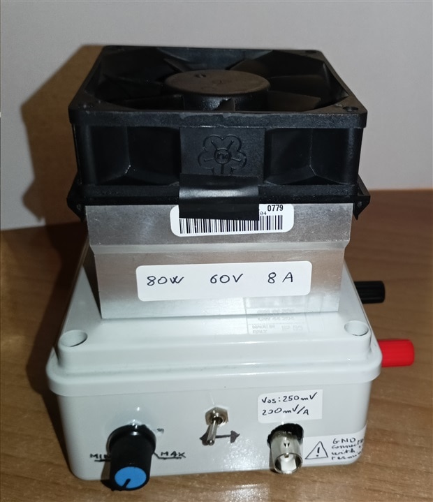
Arguably, the most important components in this project are output transistors and the heatsink. I initially looked for a  2N3055 because it has nice electrical specs (15A, up to 60V and a power dissipation capability up to 115W) but the TO-3 case makes it very inconvenient to attach to a "standard" heatsink with a flat face, so I scrapped this option. In the end I settled for an old CPU heatsink/fan (from my dad's old PC) paired with a couple of TIP122 bjts.

image
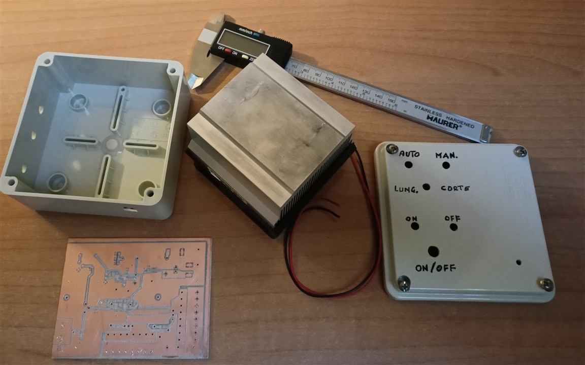
The heatsink, an used electrical box and the PCB already milled

I'm planning to power all up with an old 14V supply I have around, so as opamps I opted for LM358 because they work nicely with a single supply rail (I don't have available any rail to rail option).

The circuit

The basic circuit by itself it's quite simple: an operational amplifier with the power transistor and a shunt resistor to control the load current. This circuit will be doubled, one for each TIP122. This is not as inconvenient as it may sound, because the LM358 has two amplifiers inside the same package.

I breadboarded a test circuit to verify stability because I was not able to find any meaningful data on the TIP122 bandwidth in its datasheet. As I kind of expected, I found that it was happily oscillating. The circuit was also extremely sensitive to contact quality and external parasitic capacitances, and sometimes by touching the right spot I could make it stable. This suggests that I'm in a borderline situation and to verify it I decided to measure the frequency response of the output stage. This will give me a clearer image to appropriately compensate the circuit.

image
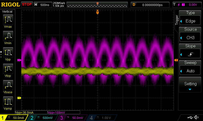
On ch3, we can see the bjt signal oscillating

image

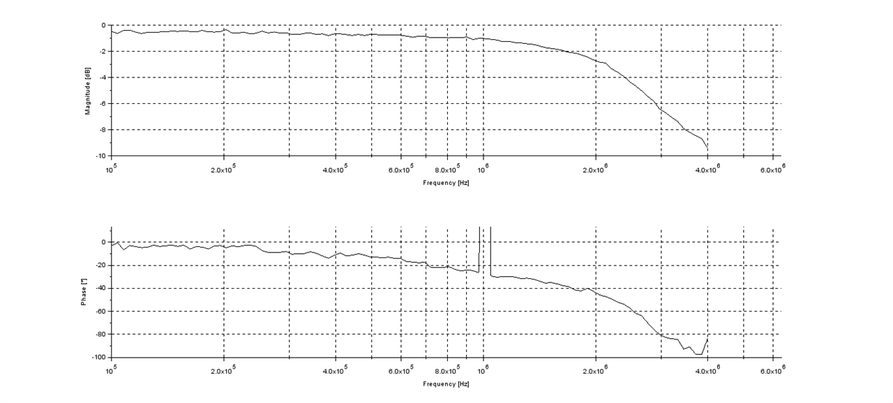
Frequency response of the TIP122 as voltage follower

This subcircuit seems to have a bandwidth around 2MHz, marginally higher compared to LM358, which exhibit a typical bandwidth of 1.1MHz.

I decided to compensate the circuit using a "noise gain" stile compensation, added a couple of comparators for overtemperature protection and a BNC connector to connect my electronic load to a function generator to create arbitrary load patterns. The final result (obtained after circuit tuning) is this:

Building it

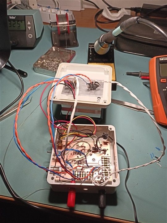
Building it included a good mixture of mechanical and electrical work that I enjoyed. I milled the pcb with my small CNC router and I opened a rectangular slot on the box top using it as well. This hole will fit the heatsink.

I manually drilled and tapped the necessary holes on the heatsink to fix my power transistors to it and to mount the heatsink itself to the enclosure. I also drilled and filed some more holes to accept connectors, switches and trimmers. I then assembled the pcb with all required components and wired all up.

image

Testing it

The first turn on is always a bit scary: will the circuit work? Or will it release the magic smoke? I found myself somewhat in between: the circuit was not working but no apparent damage either. The LDO regulator being hot was a clear signal that my 5V rail was shorted. An additional clean up from soldering and milling residues did the trick and the circuit came alive!

At DC it worked great, but the transient response showed a huge overshoot. After tuning, I managed to achieve a decent transient response, with a rise time of 6.5us and no overshoot.

image

image
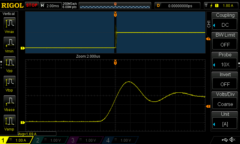
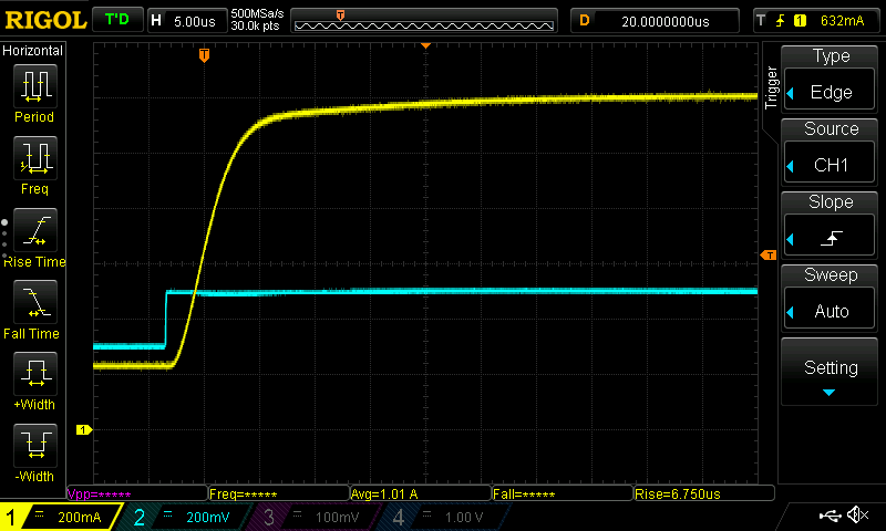
Transient response before and after tuning

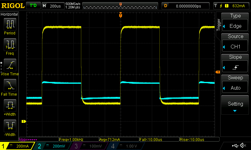
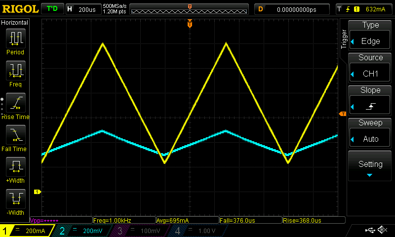
Square and triangular waves in the kHz range are no problem and it manages to replicate it on the load side quite nicely.

{gallery}My Gallery Title

image

image

I then tested its power capability, and based on bjt case temperature I decided that 80W is the max it should handle. I badged it with its specs, closed all up inside the enclosure and now I finally have an electronic load at my disposal!

image

The "fun" side: when things go the wrong direction

Yes, in the end I managed to build something that it's working, but that does not mean it's perfect or the building has been smooth. To end this blog with a "funny" note, here is a short list of things that went wrong:

  • I managed to break a drill and a screw inside the heatsink. They're still there to provide better cooling Slight smile
  • Other than causing a short circuit, during soldering I managed to melt a poor BNC connector
  • After repeatedly checking for the correct polarity, I managed to solder the trimmer backward: at the minimum position the load was drawing maximum current
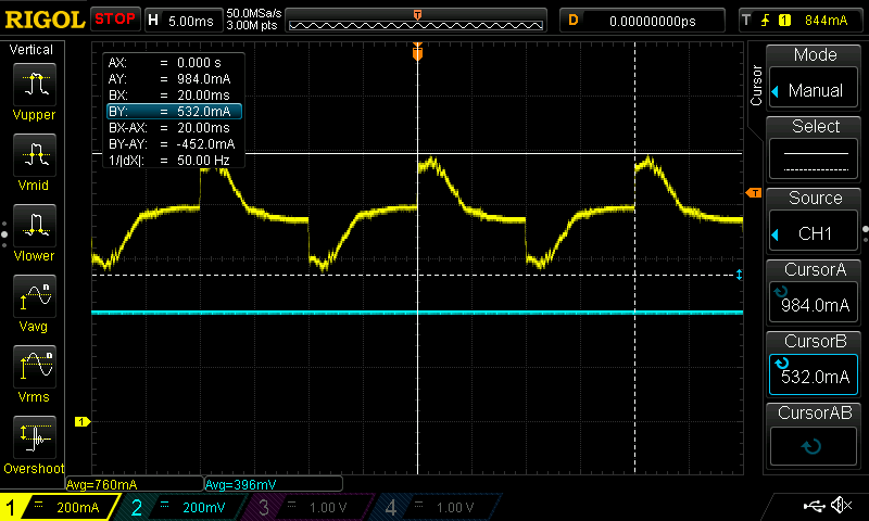
  • The power supply I choose is TERRIBLE at common mode noise. Placing 150Ω on R16 caused an output current oscillation of 450mA! It was easy to find the cause, because the noise resembles the shape of a capacitor charging after a full bridge rectifier. Replacing R16 with a short "solved" the problem
  • The same supply also managed to charge my board up to some unknown voltage (it's a floating power supply). When I came into the circuit to change a resistor for frequency response tuning, the tip of my soldering iron rapidly discharged to earth the board with a nice little blue spark. Unfortunately, the LM358 was in the way and I burned it
  • The two bjts, even if the current is evenly spread, do not heat up in the same way: one heats up to 10°C more than the other. I guess that it's probably damaged from previous usage

imageOutput current with the effect of the common mode noise. On ch2 there is the input signal

Thanks for reading!

  • Sign in to reply
  • DAB
    DAB 9 months ago

    Fun post, I always like home brew projects.

    • Cancel
    • Vote Up 0 Vote Down
    • Sign in to reply
    • More
    • Cancel
  • michaelkellett
    michaelkellett 9 months ago in reply to strb

    It's always a problem to insulate power devices from the heat sink because the insulating kits are fiddly and still compromise the coupling to the heat sink. It seems to be much more common on commercial test gear to use internal live heat sinks and a fan.

    I like the transistors or regulators that come in an insulating TO220 case - very easy to use but the thermal coupling is no better than using insulating kits. They are good for high voltages.

    MK

    • Cancel
    • Vote Up 0 Vote Down
    • Sign in to reply
    • More
    • Cancel
  • strb
    strb 9 months ago in reply to michaelkellett

    Thank you for the extremely detailed feedback. I really appreciate it.

    I completely overlooked the SOA, thank you for pointing that out! In fact I tested the 80W capabilities at 20V 4A, which is just outside of its safe region. I guess I will need to re-badge the load!

    You described extremely well circuit limitations for compensation strategy and op-amp saturation, I really can't add much more on what you already said. You made me think about the transient response, maybe the "intermediate slow down" that is visible could be reduced with your improved compensation strategy.
    image

    I would like to add another small defect of my build: the heatsink is electrically connect to bjts collector. Not the best design choice but it's fine for low voltage applications as it is intended. I just need to be careful to not short anything out by accidentally touching it.

    • Cancel
    • Vote Up 0 Vote Down
    • Sign in to reply
    • More
    • Cancel
  • michaelkellett
    michaelkellett 9 months ago

    There are a couple of problems with your design, which you may have noticed already.

    The 'tuning' scheme you have adopted reduces the feedback at low frequencies as well as high. You will get much better low frequency and DC control (and easier tuning) if you compensate the feedback loop by adding a small capacitor between the op am output and its negative input. Adjusting the value of the capacitor and the base resistor will usually allow you to tune the design by experiment and get satisfactory results. You can use power MOSFETs or even IGBTs for the power device but the Darlington transistors will be OK.

    The other thing you will find is that when there is no load connected the feedback loop will wind up the op-amp output to the power rail. If you then connect a load it will take the op-amp some time to get things under control during which a very large current will flow through the load. This is a common issue even with quite expensive commercial designs of electronic load. Having an off switch that biases the op-amp output low is a good plan - although you can still have problems if the load itself switches on and off.

    Remember is that the TIP122 can't handle 65W (what ST say in the data sheet) in real life !  But you won't be able to keep the tab on the transistor at 25C.

    With 40V across it it can only cope with about 0.75A (at 25C) = 30W, at 80V the maximum current is less than 200mA.

    image

    extract from ST data sheet

    The difference in the cooling of the transistors might be a purely mechanical thing (if one is a little bent or burred).

    Nice blog - thanks.

    MK

    • Cancel
    • Vote Up 0 Vote Down
    • Sign in to reply
    • More
    • Cancel
  • dougw
    dougw 9 months ago

    Nice job using available parts and time. An electronic load is also somewhere on my bucket list.

    • Cancel
    • Vote Up 0 Vote Down
    • Sign in to reply
    • More
    • Cancel
element14 Community

element14 is the first online community specifically for engineers. Connect with your peers and get expert answers to your questions.

  • Members
  • Learn
  • Technologies
  • Challenges & Projects
  • Products
  • Store
  • About Us
  • Feedback & Support
  • FAQs
  • Terms of Use
  • Privacy Policy
  • Legal and Copyright Notices
  • Sitemap
  • Cookies

An Avnet Company © 2025 Premier Farnell Limited. All Rights Reserved.

Premier Farnell Ltd, registered in England and Wales (no 00876412), registered office: Farnell House, Forge Lane, Leeds LS12 2NE.

ICP 备案号 10220084.

Follow element14

  • X
  • Facebook
  • linkedin
  • YouTube