Introduction
In this blog post Debugging the Turing-Welchmann Bombe I described an approach that I'd designed to take an analog signal from the Bombe and measure it over an isolation barrier. dougw suggested that an Analog Isolation Amplifier might work and I'd never heard of those before. Looking at the datasheet for the example he mentioned, I was a bit lost and it was also an extremely expensive part.
However, this part, ADuM3190 , from Analog Devices is way cheaper and looked like it could work. That's a link to uk.farnell.com so may not work in other countries but you can look up accordingly. Here's the datasheet - it describes an IC that at its simplest has is a combined ADC -> Isolator -> DAC which is pretty much most of my circuit in one IC. It has a test circuit in figure 29 on page 13 which shows an Isolated Amplifier Circuit where the output follows the input. It's a little more complicated than that, as described in "Theory of Operation" on page 14: there are two outputs, one which ranges between 0.4V - 2.4V and one which ranges from 0.6V to 4.8V (and even 5V depending upon Vdd voltage used.) For the purposes of what is required for measuring Bombe waveforms:
- A limit of 4.8V is sufficient. We used a voltage divider to bring the Bombe signal voltage to under 5V and actually around 4.7V.
- A base of 0.6V we could probably live with - and as simulation shows below that seemed to represent the 0V level of the input signal.
- 0.4V to 2.4V was more than likely to lose us too much detail in waveform shape.
What's a person to do when confronted with a new part, that might have saved quite a bit of money over the approach I took? Simulate it and fortunately, Analog Devices provides a LTSpice model to make that possible.
Caveat
I am no expert in LTSpice by any means. The results of simulations I show below may be impacted by my lack of experience with the tool. In addition, I have found that simulation results aren't always that accurate as they obviously depend on the quality of the model - I've seen some very whacky results trying to simulate some OpAmps for example. I would hope that the model provided by Analog Designs for a tool produced by Analog Designs is as accurate as the tool will allow though.
Simulation 1
Here, I test the basic setup of the amplifier:


I wasn't expecting this to actually be of use, but just to confirm the datasheet description. From the output you can see the 0.4V base and cut off at about 2.6V. However, the output is following the input which is promising
Simulation 2
Switching to the second output, I wanted to simulate what happened with a full 5V input without using a 10V pull up source.


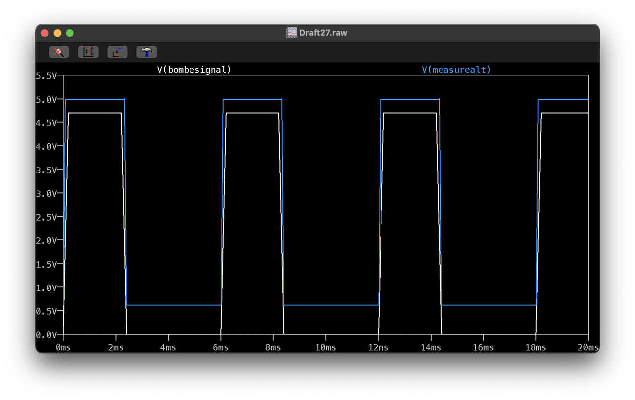
I wanted to use a 5V pull up source rather than create yet another one at 10V (as recommended by the datasheet to get a full 5V headroom.) The simulation actually shows the waveform ranging from 0.6V to the full 5V, however it's also showing that it isn't fully following the input waveform.
Simulation 3
A slight change to the previous one, I changed the pulse value to 4.7V in-line with the expected Bombe input signal.


This was interesting. It seems to indicate that the output waveform will actually give the full voltage range of the input signal if the input 0V is mapped to the output 0.6V. Still doesn't accurately follow the input waveform though.
Simulation 4
For giggles, I wondered what would happen if I injected a noisy signal into it - the Bombe is very noisy.


Sort of worked - the noise is cut off at the limits of the IC output
Simulation 5
I changed the pulse to actually delay the fall time a little more which is what I was seeing in my actual observations


At least with simulation it isn't accurately following the input signal.
Simulation 6
I wanted to see how far out the input and output signals are, at least under simulation


That's clearly a problem if right. The Bombe doesn't produce sine waves, just pulses, but I would need a solution where output traced input - my design with the broken out ADC/isolator/DAC elements does that and will follow sine waves, triangle waves and arbitrary waves without problem.
Simulation 7
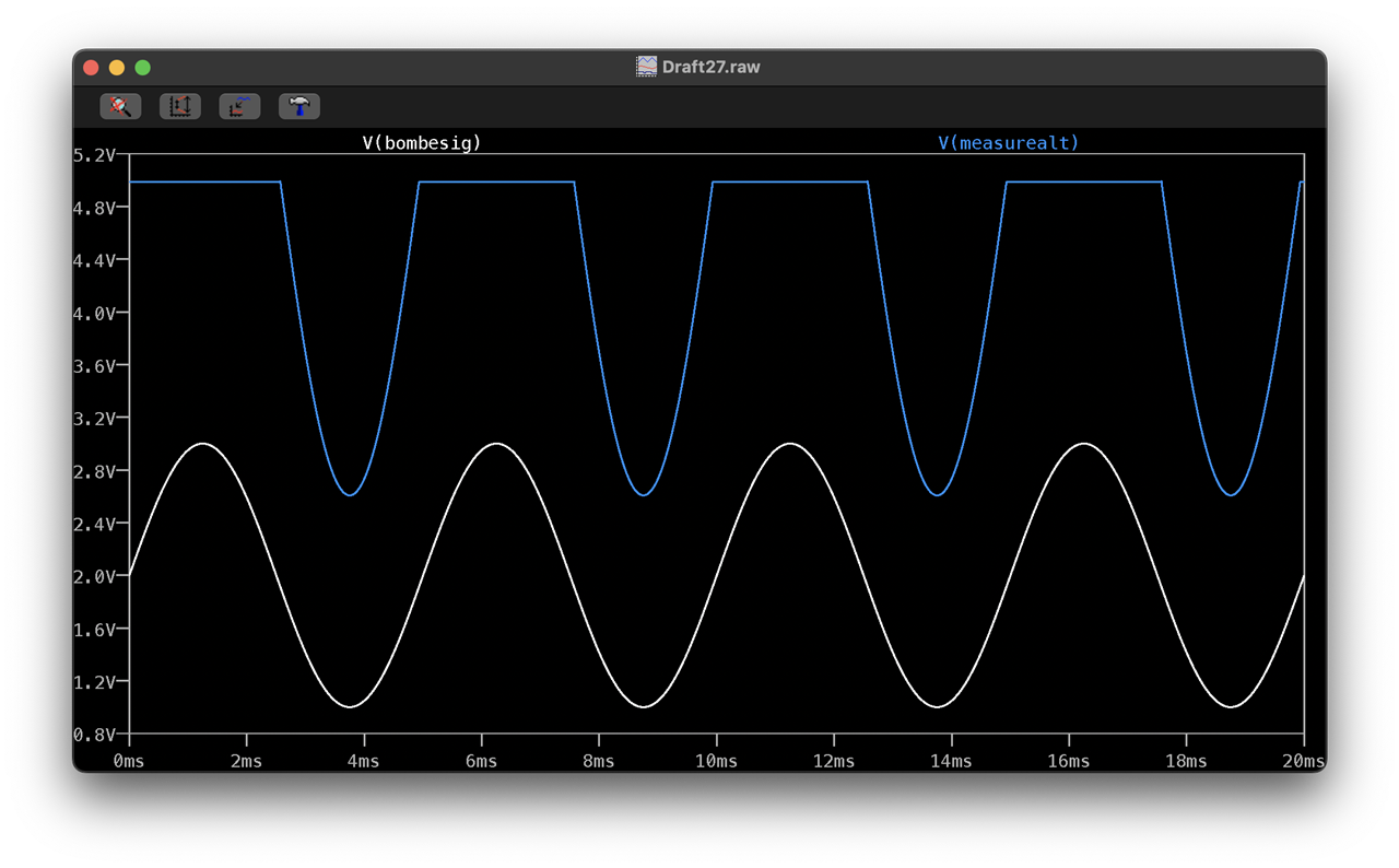
Final test - changing the sine wave so it is fully within the expected range of the IC: a 1V amplitude wave centred on 2V


Interesting and weird! It looks like the output could follow the input - at least to the extent that a curve on the output is visible. Unlike Simulation 6, there is an attempt at following the curve, clearly cut off at the 5V limit. At first thought, it looked like the model for the IC is taking the 2.0V level of the sine wave as the 'base' input voltage as the output trace drops down to 2.6V but that doesn't follow through as the upper limit would then be 2.6V + 2V = 4.6V but it's clearly cutting off at 5V.
Summary
If the simulation is accurate, I'm not sure how useful this component might actually be for my problem - the output doesn't seem to accurately reflect the input. There could be something in the datasheet that points to this perhaps and other parts might be more accurate. It's possible that my simulation circuit isn't correct.
At the very least it was worth undertaking to see how such a part might work and given its price and minimal extra components, then actually prototyping with it is possible - perhaps when I need to make another purchase I'll throw one of these in the basket.

-

shabaz
-
Cancel
-
Vote Up
0
Vote Down
-
-
Sign in to reply
-
More
-
Cancel
-

Andrew J
in reply to shabaz
-
Cancel
-
Vote Up
0
Vote Down
-
-
Sign in to reply
-
More
-
Cancel
Comment-

Andrew J
in reply to shabaz
-
Cancel
-
Vote Up
0
Vote Down
-
-
Sign in to reply
-
More
-
Cancel
Children