KiCad has always had simple tools for creating board outlines but Version 6 now allows SVG vector graphic files to be easily imported. The benefits of using SVG files include:
- Access to powerful graphic applications outside of KiCad
- Ability to use stock files from the internet
- Easy scaling with no loss of detail
This blog will focus on creating a PCB outline but in a future post, I plan to use the same drawing in a demonstration of how to add art on different layers to a PCB.
Creating SVG Files
One way of obtaining SVG art is to search for and obtain it on the internet. It is also possible to convert bit map files although they don't always convert well. I'm going to create some art using Inkscape but other tools are available. Inkscape is a free design tool that is powerful with a good online community and tutorials. The details on how to use Inkscape will be left out - I'm a beginner and suggest tutorials if you are unfamiliar with the program and wish to use it.
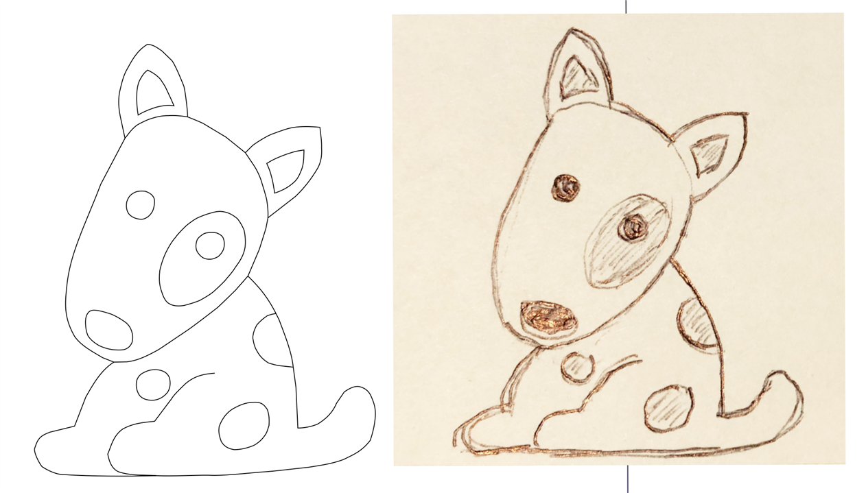
I still like to draw by hand and after looking at cartoon dogs on the internet made the quick sketch below to my tastes and photographed it with my phone (I've been doing too much cat stuff recently).

The sketch was then imported into Inkscape and the outline was traced on a new layer using the Bezier curve tool as shown below.

The remaining detail was then added to new layers.

Next, the drawing was resized although that could have been done when importing into KiCad.

Since only the outline was needed at this point, it was isolated by leaving only that layer visible. Inkscape does not appear to have an option to save a single layer (please correct me if I am wrong). After selecting the outline it was copied over into another Inkscape window that was running and saved.
EDIT: I was wrong :-) See the explanation in the comments below by javagoza for a way to export individual layers.
The image below shows the outline ready to be saved.

Creating a Board Outline in KiCad 6
From this point on, the process is the same whether the image was created as done above or downloaded off the internet.
Open up the PCB editor in KiCad. I started with a blank slate but the outline can be imported at any stage of the layout process.

Select File-->Import-->Graphics and the following dialog box will open.

Navigate to where the SVG file is located and select Edge Cuts as the Graphic layer. I've left the rest of the settings as defaults but please observe that the SVG file could have been rescaled at this point. Press OK and the image should appear.

If the image doesn't appear or looks wrong then make sure the SVG file has a closed path with no extraneous lines on it. This is how the demonstration image looks in the KiCad 3D Viewer.

Conclusion
KiCad 6 offers a much improved and simpler way of creating complicated edge cuts. In the next blog, I intend to demonstrate how additional art and electronics can be added to the PCB.

Top Comments