


This is another exploratory blog relating to bipolar junction transistors (BJTs). This time I'm going to look at saturation.
Be aware that I'm not an expert in all this: I'm studying it and you're looking over my shoulder as I experiment and explore the subject.
So this is not a tutorial and some of my explanations may, at times, be wrong.
What is saturation and why does it occur?
If you take an NPN transistor, like the 2N3904 devices I've been using in most of my experiments, and measure the base-emitter
junction using a diode test function on a multimeter, it behaves like a silicon diode (that's because it is one). We're used to that diode
because we are conscious of it when we design. If we were to probe a bit further, we'd discover that there's also a diode from the base
to the collector. That diode is a little less visible to us because when the transistor is operating with a reasonable collector voltage it is
reverse-biased and doesn't affect the operation too much (technically, it certainly does affect the ac operation, because the capacitance
across that junction is one of the things that limits the high frequency performance, but that's not where I'm going with this blog).
The forward voltages of those two diodes are slightly different (for a 2N3904, I see a difference of about 20mV at whatever the test
current is). That's because the properties of the collector and the emitter regions are different - the emitter is more heavily doped than
the collector.
So, is this just of academic interest? Well, no. Let's think what happens as the collector voltage falls and comes closer to the emitter
voltage. At some point the base-collector diode is going to cease to be reverse biased and at that point the operation of the transistor
starts to change. The neat self-regulation that the transistor does, where the collector current is proportional to the base current starts
to fall down. The base current will no longer simply relate to the collector current and we can keep increasing the base current without
it further affecting the collector current. This is about as far as I can go with an explanation at the moment - I'm not good enough with
the solid-state physics that underpins transistor operation to be sure of the mechanism and describe it properly.
A side-effect of that whole process is that charge starts to accumulate in the transistor. It's that accumulation that the term 'saturation'
comes from. It doesn't do any harm but there is an important consequence if you are a designer - the device will remain on for some
time, even if you remove the base current (ie if you are using the transistor as a switch it will be slow to turn off - 'slow' here means
hundreds of nanoseconds for the kind of transistors I've been experimenting with, so no problem at all if you are switching a relay
but much more of a problem if it's supposed to be a logic switch). The way to get around that, if you did want fast switching, is to drag
the charge back out again rather than wait for the normal transistor action to use it up.
So, when we talk of a transistor 'saturating' or 'going into saturation', we are referring to a consequence of what happens, rather than
the direct cause. [I guess people saying 'the transistor has saturated' was more natural than saying 'the base-collector diode of the
transistor has ceased to be reverse biased'.]
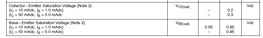
Because the base current can now continue increasing without a change in the collector current, the manufacturer has to be careful
to specify the relationship between the two when giving saturation voltages on a datasheet. The standard that manufacturers seem
to have settled on is to have the base current a tenth of the collector current (I imagine that was chosen to be safely underneath the
minimum gain that a large power transistor might have at high current, a figure of perhaps 40 or 50). Here's an example from a
2N3904 datasheet where they give indicative voltages for two different collector currents
They also give this handy graph and it's that that I'm going to have a go at replicating in the next section.

That graph is very useful because, as well as showing the Vbe(sat), they also give a second curve for the Vbe with the collector
held at 1V where the transistor is out of saturation. That shows us the difference the saturation makes. It also emphasises something
that I'm going to skate around here and that is that, at high currents, there is also an ohmic component from the bulk resistivity of the
semiconductor [at low currents, the Vbe voltage increases at about 60mV per decade of current (it should be a straight line on the
graph with its log scale for current), but at high currents it increases faster because of that additional factor]. The collector current
will also be affected by the same kind of ohmic effect.
Measuring Saturation Voltages
I'm now going to try measuring Vce(sat) and Vbe(sat) over a range of collector currents. Here's the simple circuit I've come up with.
There's a quad, precision op amp to run a constant current into each of the base and the collector. The respective currents will be in
the ratio 1:10 [the two current sources are identical except for the current-sense resistor which sets the relationship between the
voltage at the input and the current generated].

I'm going to have a 0V to 2V ramp from a function generator going in and adjust the oscilloscope so that it displays over the width of
the screen (I'm using the sync output from the generator to trigger the 'scope). The 2V input corresponds to 200mA in the collector
and 20mA in the base. That way the 'scope will draw the graph for me with the horizontal scale being equivalent to 0-200mA at the collector.
Here it is wired up on a breadboard (almost as messy as the circuit!):

Here are the resulting curves for a 2N3904 transistor (yellow base voltage, blue collector voltage):
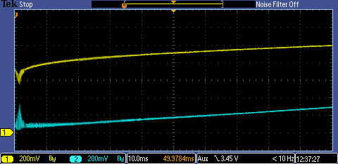
It wasn't all that stable. My function generator is noisy, which doesn't help. Including a simple RC filter at the input helped cut down the noise
going in. I also added capacitors across the feedback resistors to the differential amplifier outputs to compensate the op amps more. Something
else that helped was giving the amplifier a negative rail. In spite of that, the transistor hoots a bit under some circumstances but, if you ignore
the area up to about 20mA collector current (the first horizontal division), the rest looks reasonable. In the simulator it's stable, so I'm probably
looking at the way three rf transistors interact on a real, messy, plug-in breadboard.
The Vce(sat) extends from just below 100mV at 20mA up to just below 300mV at 200mA collector current. The Vbe(sat) is higher than you
would see for operation out of saturation and goes from about 800mV at 20mA collector current to just over a volt at 200mA.
My curve looks different to theirs, but that's largely due to my having a linear scale for the current - if you pick a few spot values and compare,
there's not too much difference. One important difference between the way I'm doing this test and the way a manufacturer would it is that they
use a pulse test where the transistor is only on for 2% of the time. That removes the temperature effects from the otherwise high dissipation
at the higher end of the scale.
Here are the results for a 2N30532N3053 part. This is a somewhat slower device (fT = 100MHz) and is much more stable on my test setup.
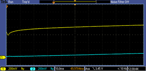
In this case, the Vce(sat) at 200mA collector current is much less, being slightly over 100mV. Vbe(sat) is also lower, being about 850mV.
If you found this interesting and would like to see more blogs I've written, a list can be found here: jc2048 Blog Index
Top Comments