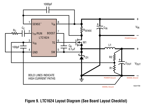
Hopefully someone can take a look and help me get some insight into what is being stated. This is in relation to layout of a DC-DC switching regulator LTC1624 (for my power supply build). The data sheet, pages 20 and figure 9 on page 21, seem to conflict or, at least, not make sense in respect to the reference made to power and signal grounds.
Layout instructions state:
- Power ground and signal ground must be segregated.
- Ground pin of LTC1624 must return to -ve of Cout.
- The resistive divider must connect between +ve of Cout and signal ground
- Cin must connect to Vin and Ground of LTC1624
(I've summarised somewhat but that's the essential gist - they make reference to a POWER ground and a SIGNAL ground).
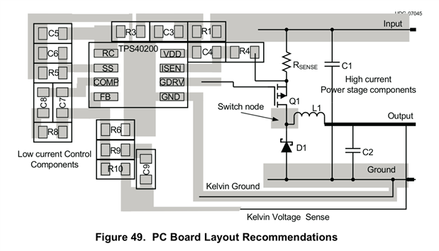
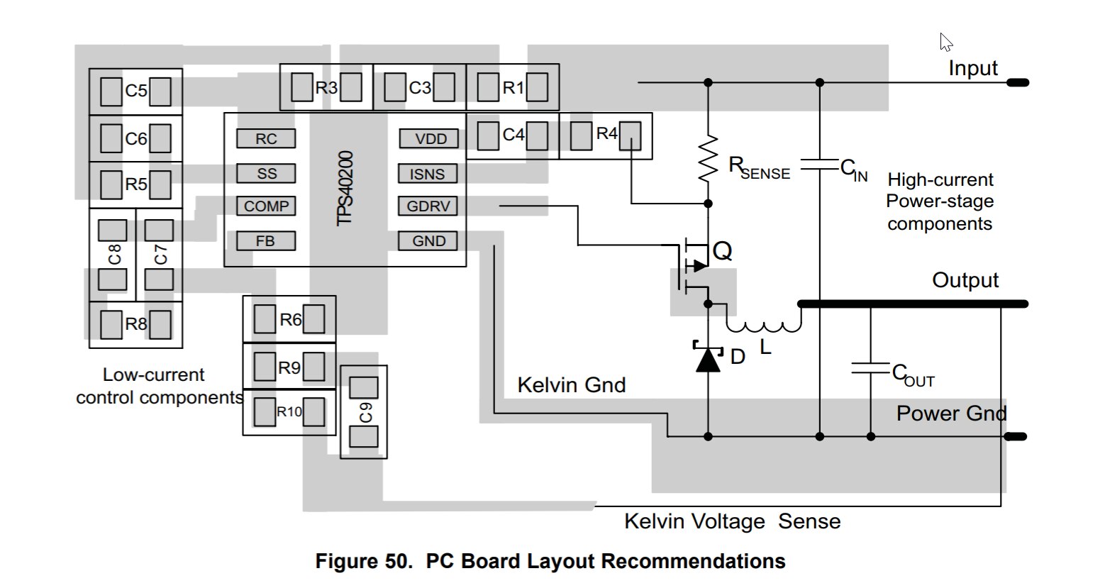
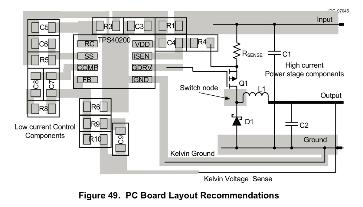
Figure 9:

Looking at the layout figure 9, you can see that it follows these instructions and it would imply that -ve of Cout is signal ground; however this is directly linked to Schottky -ve pin, Cin-ve and back to the Vin - terminal
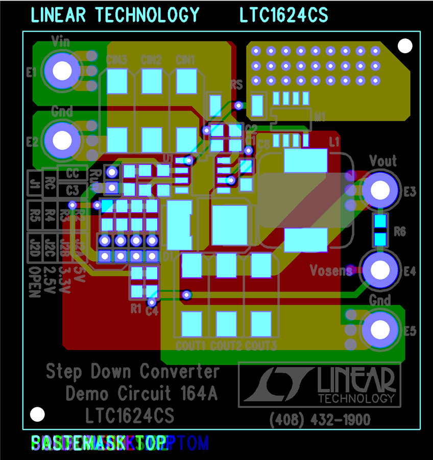
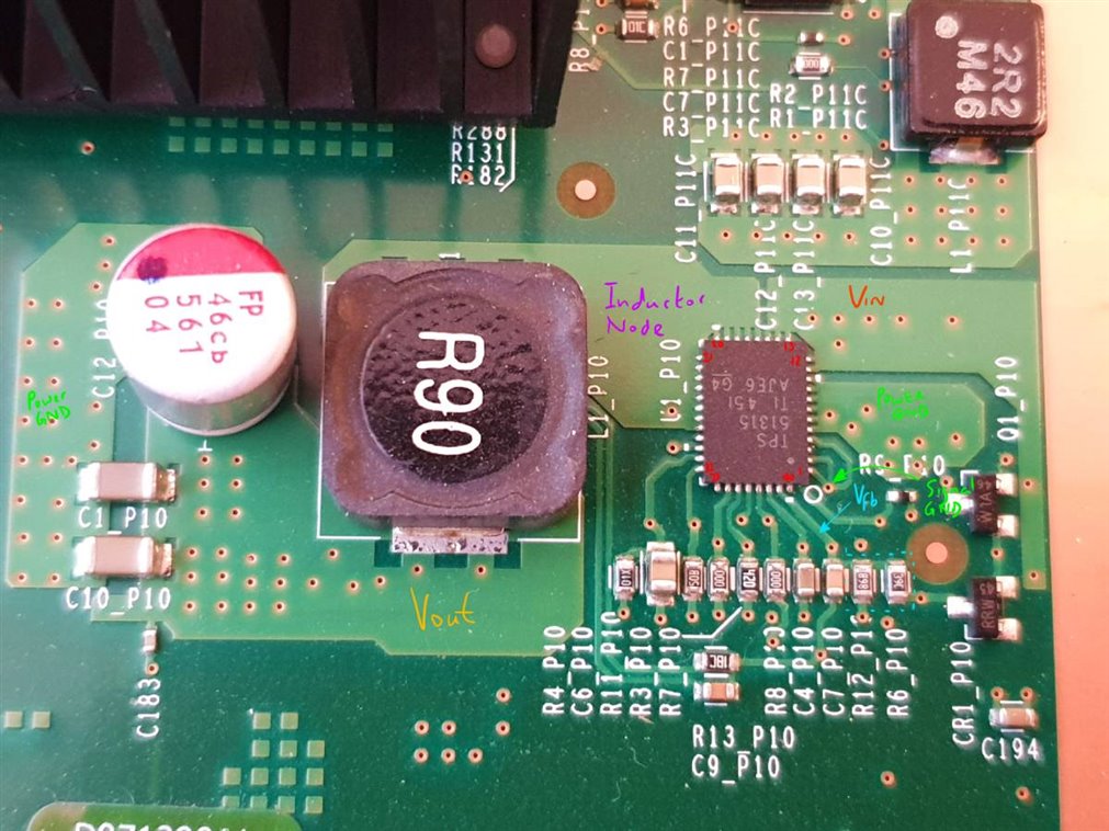
I've found a demo board for this chip. Unfortunately, the gerbers don't load into any viewer I can find, but there are images here on page 8 (last page.)
Silk Screen:

Component Side (top):
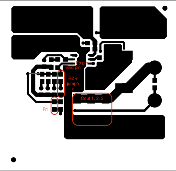
Solder Side (bottom):

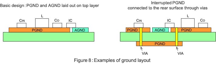
Looking at the Component Side (top) and Solder Side (bottom), there are two ground planes: a 'Z' like structure from Vin GND terminal E2, top left, under the LTC1624, to the Vout GND out terminal bottom right E5; the biggest copper area on Solder Side is Ground, also tied into E2 and E5. I know 'Z' ground isn't a technical term but bear with me - I want to call it POWER ground but I'm not sure that would be right! Looking at the Component Side silkscreen, it is clear Cout -ve is tied to the component side 'Z' ground; the feedback divider is also connected to the 'Z' ground where the sideways-U trace is. It's worth noting also that the loop compensating resistor/capacitor is tied to the 'Z' ground.
Looking at Figure 9 and the PCB layout, it would seem that everything is tied into the same ground - it isn't clear if anything is tied into the ground plane on the Solder Side (except at terminals E2 and E5) and I've traced every component that has a ground connection to the Component Side 'Z' ground. In other words, it's not clear what they mean by tying the resistor divider to signal ground.
Anyone who has been following along with my build will know I've right-royally screwed up the grounding and layout and I don't want to do it again. It's been clear that I've not fully understood how Switching Regulators work so I've been doing a lot of reading and now have a better idea. I understand why the feedback divider should stretch across Cout so why it is tied to the -ve of Cout and figure 9 actually makes sense to me (except for the ground symbol under the Schottky plus a link to Vin GND.) What doesn't make sense are the layout instructions reference to Power and Signal grounds and the layout of their PCB - it would seem that the way both the feedback and compensation components are tied to the ground plane, right by Schottky, would be inviting noise and poor behaviour. It's also tying noise onto the Vout GND terminal as well.
I'd have to assume that the PCB layout is purely for the purposes of demonstrating the functionality of the LTC1624 and is less concerned with the quality of the output. Thus, I would expect that I would tie the Feedback and LTC1624 grounds to Cout -ve along a different Ground route. That would also be the point for tying downstream ground components (so basically, like Figure 9 where the Vout -ve is deemed signal ground and Cout -ve becomes the star ground point for signal.)
Is this clear to anyone else?